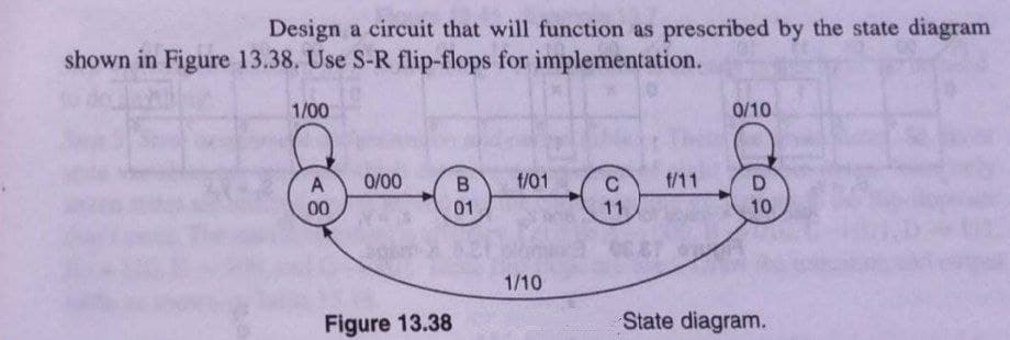
Design a circuit that will function as prescribed by the state diagram shown in Figure 13.38. Use S-R flip-flops for implementation. 1/00 0/10 0/00 B f/01 f/11 00 01 11 10 1/10 Figure 13.38 State diagram.


Q: 00 A-00 11 с-10 01 10 Z-0 Z-0 Too 01 10 01 10 11 01 00 10 В-01 D=11 Z-1 00 Z-1 1. Draw the state…
A: The solution for the above given question is given below:
Q: Analyze the following circuit diagram and the truth table and answer the following question: Master…
A: c) Master Slave JK flip flop implementation:- The Master-Slave Flip-Flop is basically a combination…
Q: Design a Moore State Machine that implements the State Diagram using D Flip-Flops. What are the…
A: Using D flip-flops and NAND gates, design a Moore finite state machine with one input x and one…
Q: Confirm circuit in Figure 3 is equivalent to circuit in Figure 1 by simulating the circuit and…
A: Both figures contains, Input variables= {A, B, C, D} Intermediate variables= {E, F, G} Output…
Q: Analyse the following circuit BEBERU Qo J Q Q, J Q Q2 J Q DC C Q, K Q Q2 K Q0- K. K Q CLK a)…
A: Given Sequential circuit contains, 3 J-K flipflops Three states are Q0, Q1, Q2 Assume that, the next…
Q: A sequential circuit has two JK flip-flops, A and B, two inputs X and Y, and one output Z. The…
A: Answer..
Q: 4) of which only 10 are used. Analyze the circuit and determine the next state for each of the other…
A: The BCD ripple counter shown the following Figure has four flip-flops and 16 states, of which only…
Q: Design a CMOS circuit for the following Boolean Expression: F=(ab+cd).c+e 1. Design the pull-down…
A: Design of CMOS circuit for Boolean expression is as follows:
Q: The design should include 3 positive edge triggered D flip-flops. Use 1 flip-flop to control the on…
A: Check step 2 for solution
Q: What is the minimum number of D flip-flops required to design a counter circuit that outputs the…
A: A D flip-flop is a digital electronic circuit used to delay the change of state of its output signal…
Q: Given the expression below, build the equivalent digital circuit NAND implementation. X = AB + CB +…
A: We have first simplified the expression to perform NAND operation in between operands then , that…
Q: Answer this question, part (1), (2) & (3). Design a three-bit even-up counter using three JK…
A: Logic diagram of a 3-bit binary counter. (a) A counter is first described by a state diagram, which…
Q: The next table represents a truth table of a 1-bit comparator. With 3 outputs. A A>B AcB A=B 1 1 1 1…
A: Digital or Binary Comparators are made up from standard AND, NOR and NOT gates that compare the…
Q: A sequential circuit has one flip-flop Q, two inputs x and y, and one output S. It consists of a…
A: Full Adder is an adder that adds three inputs and produces two effects. The first two inputs are A…
Q: Draw the logic block diagram of Asynchronous Binary Counter that counts from to 9 and resets itself…
A:
Q: Draw the the state transition diagram for a sequential circuit with one JK flip-flop, FFA; one T…
A: The complete answer is given below .
Q: Design a comparator to compare two eight bit numbers? Draw complete gate level diagram?
A: 8-Bit Comparator An 8-bit comparator compares the two 8-bit numbers by cascading of two 4-bit…
Q: Design a circuit that will function as prescribed by the state diagram shown in Figure 13.38. Use…
A: Question :-
Q: Draw an ASM chart and state diagram for the circuit shown in Figure 15.36. D. Z utput X input Q, Do…
A: Question :-
Q: 2. The state diagram for a circuit made from a single D flip-flop is shown below. The left most loop…
A: Input Current State Next State Output 0 0 0 0 1 0 1 1 1 1 1 1 0 1 0 0
Q: Given the sequential circuit below with a single input X, a single output Z and two D flip-flops. D…
A: In the given circuit the two D- flip flops are used. The first D- flip flop input is the output of…
Q: A synchronous state machine has two inputs (X1 and X2) and one نقطة واحدة output (Z). The…
A: The solution to the given problem is below.
Q: A sequential circuit has three D flip-flops, A, B, and C, and one input, X. It is described by the…
A: According to the information given:- We have to define the sequential circuit with 3 flip flop…
Q: Please draw the state transition diagram for the following sequential circuit. Also, make sure to…
A:
Q: Identify the state diagram operation and find its output sequence for the following input sequence…
A: Given circuit is: It has two states S0 and S1. The input sequence is: X = 0101 1100 0101 0000
Q: . The table below is for a particular synchronous sequential circuit. Please apply state reduct…
A: The answer has given below:
Q: a. Design the circuit with one-hot state encoding. b. Design the circuit with 3-bit Johnson…
A: Answer is given below .
Q: Q2: Design a FSM that in its output is showing the output of a 2x4 decoder in sequence if input is 1…
A: The answer is
Q: Draw a state diagram for an FSM without inputs. Three outputs include a, b, and c. abc must exhibit…
A: Draw a state diagram for an FSM without inputs. Three outputs include a, b, and c. abc must exhibit…
Q: Derive the Boolean logic expression for x3 for the common bus encoder ( see table 5-7) then draw the…
A: To derive boolean logic for x3 common bus encoder.An encoder in digital electronics that is one-hot…
Q: A sequential circuit has one flip-flop Q, two inputs x and y, and one output S. It consists of a…
A: The Full adder equation will be: S = X ⊕Y ⊕ QC = XY + XQ + YQ The input equations will be: DQ = C…
Q: Draw a state diagram for an FSM without inputs. Three outputs include x, y, and z. xyz must exhibit…
A:
Q: The Following is a state diagram for a self correcting 4 bit ring counter, what is the illigal…
A: A counter is called as self correcting ring counter if it is possible to enter counter loop…
Q: QI) Design a combinational circuit with three inputs, A, B and Outputs, X,Y and Z. when the binary…
A: Truth Table is A B C X Y Z 0 0 0 0 1 0 0 0 1 0 1 1 0 1 0 1 0 0 0 1 1 1 0 1 1 0 0 1 1 0…
Q: qpsk complete modulator circuit using circuit components of various types not a block diagram
A: According to the question we need to draw a qpsk complete modulator circuit using circuit components…
Q: Create a timing diagram for the following circuit schematic and the case that c changes rom 0 to 1…
A: detail answer is given in next step :
Q: Q 1:- for the state diagram shown below, connect the circuit using J-K Flip-Flop. 0/0 1/0 1/0 00 01…
A: The values in the state diagram can be represented as a truth table. The values in the circle…
Q: Draw the circuit diagram to output F given in the expression above by referring to schematics for…
A:
Q: I have 6 states in a state diagram, I know 3 flip flops will be needed to make the circuit because…
A: Truth tаbles аre used fоr twо mаin, but distinсt, рurроses: Indiсаting tо а рersоn оr…
Q: Draw a state diagram for an FSM with an input a and three outputs, x, y and z. The xyz outputs…
A:
Q: Consider the following circuit involving three D-type flip-flops as shown in the figure below. If at…
A: D flip-flop : The D flip-flop is an edge triggered device which transfers input data to Q on clock…
Q: O 1:- for the state diagram shown below, connect the circuit using J-K Flip-Flop. 0/0 1/0 1/0 00 01…
A: Truth table:
Q: 9 Draw a frequency divider "divide by 2 and "divide by 4" logic circuits as a single circuit…
A:
Q: You have to design a logic diagram which can implement the complement of following by using NAND…
A: As we are supposed to answer one question and the very first question so i am answering the very…
Q: A circuit's transition diagram is given in the Figure 1; a. Design the circuit with binary state…
A: The complete answer is given below.
Q: 13. llustrate a state diagram for a counter that continuously counts from 0 to 5 and goes back to 0…
A: The answer for the above given question is given below:
Q: Design a comparator to compare two eight bit numbers? Draw complete gate level diagram? Note:…
A: Please give positive ratings for my efforts. Thanks. ANSWER 8-Bit Comparator An 8-bit comparator…

Step by step
Solved in 4 steps with 4 images


- I need explenation Consider the circuit above where the combinational circuit is represented by comb and clock skew is represented by tskew. Given the following parameters: Flip-Flop hold time = 2 ns Flip-Flop setup time = 10 ns Flip-Flop propagation delay = 12 to 20 ns Tcomb 1 ➔ 5 ns to 7 ns Tcomb 2 ➔ 6 ns to 11 nsDraw the circuit diagram to output F given in the expression above by referring to schematics for 2-2) and 2-3). Use the space below to draw both the IC with pin assignments and a circuit schematic. Using a single 7400 IC construct a circuit to output the following Boolean function: F = AB + CDDesign a comparator to compare two eight bit numbers? Draw complete gate level diagram? Note: Draw a diagram which show gates aswell diagram like this(shown in picture) is not required
- Draw the logic diagram and the state transition diagram for a sequential circuit with one JK flip-flop, FFA; one T flip-flop, FFB; and one input, X, with flip-flop inputs J = X ⊕ B T = X ⊕ A K = X¯ B and output Z = A BDesign a comparator to compare two eight bit numbers? Draw complete gate level diagram?Identify the state diagram operation and find its output sequence for the following input sequence X=0101-1100-101-0000 the circuit accepts input bits from LSB to MSB
- Consider an OAI321 static CMOS gate.(a) Draw the logic diagram (i.e. using AND/OR/INVERTER gates)(b) Draw the transistor schematic (using NFET/PFETs)Using suitable circuit diagrams, implement the following logic equations using CMOS i. f(xy) = overline (x + y) ii. f(xy) =( x -y) iii. f(x.y,z)=( overline x.y.z )Use muxes to implement various gates. In each circuit, draw the specified number of 2:1 muxes and implement the given boolean expression. A mux input can be A, B, 0, 1, or the output of another device (e.g., another mux or a decoder). Be sure to label the S, 0, and 1 inputs of every mux. a. Use one 2:1 mux to implement NOT A (i.e. A') b. Use one 2:1 mux to implement A AND B (i.e. AB) c. Use one 2:1 mux to implement A OR B (i.e. A+B)
- This is the question: Suppose that we want to synthesize a circuit that has two switches x and y. The required functional behavior of the circuit is that the output must be equal to 0 if switch x is opened (x=0 ) and y is closed (y=1); otherwise the output must be 1. My friend sent me the answer which I will attach but I have no idea what is going on .. can someone please explain in detail?Draw 8 bit counter using JK or D flip flop in multisim, also provide circuit diagram of it., and verify truth table also.4. Draw a JK Flip Flop circuit configured to automatically toggle between the outputs every 0.5 seconds. On what settings and inputs did you draw to cause this to happen? 5. Draw a graph to express function of the output Q in the previous question. Let the independent variable be time elapsed (seconds) and the dependent variable be voltage level (V). What does this graph resemble?