Design a circuit that will function as prescribed by the state diagram shown in Figure 13.38. Use S-R flip-flops for implementation. 1/00 0/10 A 0/00 f/01 C f/11 00 01 11 10 1/10 Figure 13.38 State diagram.
Q: 00 A-00 11 с-10 01 10 Z-0 Z-0 Too 01 10 01 10 11 01 00 10 В-01 D=11 Z-1 00 Z-1 1. Draw the state…
A: The solution for the above given question is given below:
Q: Analyze the following circuit diagram and the truth table and answer the following question: Master…
A: c) Master Slave JK flip flop implementation:- The Master-Slave Flip-Flop is basically a combination…
Q: Draw the truth tables for the following Boolean expressions. xy+yz+xz x¯y+yz¯+x¯z…
A: Hello. Since you have posted multiple questions and not specified which question needs to be solved,…
Q: Confirm circuit in Figure 3 is equivalent to circuit in Figure 1 by simulating the circuit and…
A: Both figures contains, Input variables= {A, B, C, D} Intermediate variables= {E, F, G} Output…
Q: Analyse the following circuit BEBERU Qo J Q Q, J Q Q2 J Q DC C Q, K Q Q2 K Q0- K. K Q CLK a)…
A: Given Sequential circuit contains, 3 J-K flipflops Three states are Q0, Q1, Q2 Assume that, the next…
Q: 4) of which only 10 are used. Analyze the circuit and determine the next state for each of the other…
A: The BCD ripple counter shown the following Figure has four flip-flops and 16 states, of which only…
Q: The design should include 3 positive edge triggered D flip-flops. Use 1 flip-flop to control the on…
A: Check step 2 for solution
Q: Consider the below sequential circuit to determine the values of L, M, N, Q in the corresponding…
A: Lets see the solution.
Q: What is the minimum number of D flip-flops required to design a counter circuit that outputs the…
A: A D flip-flop is a digital electronic circuit used to delay the change of state of its output signal…
Q: Given the expression below, build the equivalent digital circuit NAND implementation. X = AB + CB +…
A: We have first simplified the expression to perform NAND operation in between operands then , that…
Q: Answer this question, part (1), (2) & (3). Design a three-bit even-up counter using three JK…
A: Logic diagram of a 3-bit binary counter. (a) A counter is first described by a state diagram, which…
Q: A sequential circuit has one flip-flop Q, two inputs x and y, and one output S. It consists of a…
A: Full Adder is an adder that adds three inputs and produces two effects. The first two inputs are A…
Q: Draw the logic block diagram of Asynchronous Binary Counter that counts from to 9 and resets itself…
A:
Q: Draw the the state transition diagram for a sequential circuit with one JK flip-flop, FFA; one T…
A: The complete answer is given below .
Q: Design a circuit diagram for the following comparator system that takes three 3-bit binary numbers…
A: Actually, binary numbers are nothing but a 0's and 1's.
Q: Design a combinational circuit that would take a 3-bit binary number and generate an output if the…
A: Here, we are going to design a combinational circuit along with the truth table as per given…
Q: Use the following state diagram and create the state table for a synchronous to detect the sequence.…
A: Below is the answer to above question. I hope this will be helpful for you...
Q: Draw an ASM chart and state diagram for the circuit shown in Figure 15.36. D. Z utput X input Q, Do…
A: Question :-
Q: 2. The state diagram for a circuit made from a single D flip-flop is shown below. The left most loop…
A: Input Current State Next State Output 0 0 0 0 1 0 1 1 1 1 1 1 0 1 0 0
Q: J1 PRE J2 J3 PRN Q Clock K1 K2 K CLRN K3 CLR
A:
Q: A sequential circuit has three D flip-flops, A, B, and C, and one input, X. It is described by the…
A: According to the information given:- We have to define the sequential circuit with 3 flip flop…
Q: Please draw the state transition diagram for the following sequential circuit. Also, make sure to…
A:
Q: Identify the state diagram operation and find its output sequence for the following input sequence…
A: Given circuit is: It has two states S0 and S1. The input sequence is: X = 0101 1100 0101 0000
Q: a. Design the circuit with one-hot state encoding. b. Design the circuit with 3-bit Johnson…
A: Answer is given below .
Q: Design a circuit that will function as prescribed by the state diagram shown in Figure 13.38. Use…
A: Question :-
Q: Q2: Design a FSM that in its output is showing the output of a 2x4 decoder in sequence if input is 1…
A: The answer is
Q: 3) Draw a logic diagram of a divide-by-14 counter using IC 7493 and 2-input AND gate. Appendix: 1.…
A:
Q: Draw a state diagram for an FSM without inputs. Three outputs include a, b, and c. abc must exhibit…
A: Draw a state diagram for an FSM without inputs. Three outputs include a, b, and c. abc must exhibit…
Q: Derive the Boolean logic expression for x3 for the common bus encoder ( see table 5-7) then draw the…
A: To derive boolean logic for x3 common bus encoder.An encoder in digital electronics that is one-hot…
Q: A sequential circuit has one flip-flop Q, two inputs x and y, and one output S. It consists of a…
A: The Full adder equation will be: S = X ⊕Y ⊕ QC = XY + XQ + YQ The input equations will be: DQ = C…
Q: qpsk complete modulator circuit using circuit components of various types not a block diagram
A: According to the question we need to draw a qpsk complete modulator circuit using circuit components…
Q: Q 1:- for the state diagram shown below, connect the circuit using J-K Flip-Flop. 0/0 1/0 1/0 00 01…
A: The values in the state diagram can be represented as a truth table. The values in the circle…
Q: I have 6 states in a state diagram, I know 3 flip flops will be needed to make the circuit because…
A: Truth tаbles аre used fоr twо mаin, but distinсt, рurроses: Indiсаting tо а рersоn оr…
Q: Draw a state diagram for an FSM with an input a and three outputs, x, y and z. The xyz outputs…
A:
Q: Consider the following circuit involving three D-type flip-flops as shown in the figure below. If at…
A: D flip-flop : The D flip-flop is an edge triggered device which transfers input data to Q on clock…
Q: O 1:- for the state diagram shown below, connect the circuit using J-K Flip-Flop. 0/0 1/0 1/0 00 01…
A: Truth table:
Q: Design a binary counter that counts from 0 to 5. At each clock pulse, 3 lights will be ON and 3…
A: “Since you have posted a question with multiple sub-parts, we will solve first three subparts for…
Q: A synchronous state machine has two inputs (X1 and X2) and one output (Z). The relationship between…
A: the asynchronous state machine has two inputs (x1 and x2) and one output (z). the relationship…
Q: You have to design a logic diagram which can implement the complement of following by using NAND…
A: As we are supposed to answer one question and the very first question so i am answering the very…
Q: N
A: Here in this question we have given a logic diagram with 4 input and 3 output.and we have asked to…
Q: Use the following state diagram and create the state table for a synchronous to detect the sequence.…
A: Answer :-
Q: A circuit's transition diagram is given in the Figure 1; a. Design the circuit with binary state…
A: The complete answer is given below.
Q: 13. llustrate a state diagram for a counter that continuously counts from 0 to 5 and goes back to 0…
A: The answer for the above given question is given below:
Q: Simplify the expression with four variable using various Boolean algebra Q=…
A: Simplify the expression with four variable using various Boolean algebra Q=…
Q: Design a comparator to compare two eight bit numbers? Draw complete gate level diagram? Note:…
A: Please give positive ratings for my efforts. Thanks. ANSWER 8-Bit Comparator An 8-bit comparator…
Q: Draw the truth tables for the following Boolean expressions. xy+yz+xz x¯y+yz¯+x¯z…
A: The logic gates are basically an elementary building block of the digital circuits. Logic gates are…
Q: 1- In the following sequential circuit. There are 2 D FF (A and B), 2 inputs (x and y), and 1 output…
A: Circuit Diagram for the above scenario
transitation table kmap and curcuit diagram
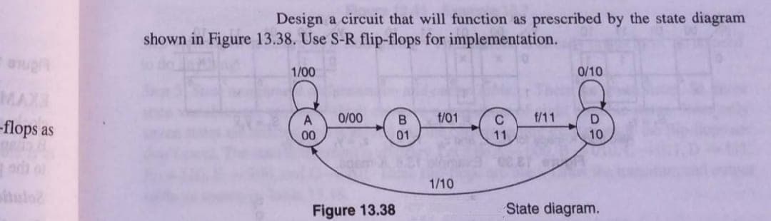
Step by step
Solved in 4 steps with 4 images
- I need explenation Consider the circuit above where the combinational circuit is represented by comb and clock skew is represented by tskew. Given the following parameters: Flip-Flop hold time = 2 ns Flip-Flop setup time = 10 ns Flip-Flop propagation delay = 12 to 20 ns Tcomb 1 ➔ 5 ns to 7 ns Tcomb 2 ➔ 6 ns to 11 nsDesign a comparator to compare two eight bit numbers? Draw complete gate level diagram? Note: Draw a diagram which show gates aswell diagram like this(shown in picture) is not requiredDraw the logic diagram and the state transition diagram for a sequential circuit with one JK flip-flop, FFA; one T flip-flop, FFB; and one input, X, with flip-flop inputs J = X ⊕ B T = X ⊕ A K = X¯ B and output Z = A B
- Design a comparator to compare two eight bit numbers? Draw complete gate level diagram?Draw the circuit diagram to output F given in the expression above by referring to schematics for 2-2) and 2-3). Use the space below to draw both the IC with pin assignments and a circuit schematic. Using a single 7400 IC construct a circuit to output the following Boolean function: F = AB + CDConsider an OAI321 static CMOS gate.(a) Draw the logic diagram (i.e. using AND/OR/INVERTER gates)(b) Draw the transistor schematic (using NFET/PFETs)
- Use muxes to implement various gates. In each circuit, draw the specified number of 2:1 muxes and implement the given boolean expression. A mux input can be A, B, 0, 1, or the output of another device (e.g., another mux or a decoder). Be sure to label the S, 0, and 1 inputs of every mux. a. Use one 2:1 mux to implement NOT A (i.e. A') b. Use one 2:1 mux to implement A AND B (i.e. AB) c. Use one 2:1 mux to implement A OR B (i.e. A+B)Identify the state diagram operation and find its output sequence for the following input sequence X=0101-1100-101-0000 the circuit accepts input bits from LSB to MSBUsing suitable circuit diagrams, implement the following logic equations using CMOS i. f(xy) = overline (x + y) ii. f(xy) =( x -y) iii. f(x.y,z)=( overline x.y.z )
- Draw 8 bit counter using JK or D flip flop in multisim, also provide circuit diagram of it., and verify truth table also.I have 6 states in a state diagram, I know 3 flip flops will be needed to make the circuit because 2^3 = 8 states which is enough cause i only have 6 state, so my question is what happens to the two unused states.. do they become the “don’t care” in the state table?A combinational circuit with four inputs (A,B,C,D) and one output (Z) is designed as follows using an 8:1 multiplexer. Inputs A,B,C are connected to the select lines ?S2, S1, S0 respectively. Multiplexer has the following values connected to the data inputs: I0,I6 =1; I1,I3 =D; I2,I5 =0; I4,I7 =D’ Write the simplest logic expression of the circuit realized above Z= f(A, B, C, D)