EXERCISE Design a combinational circuit by using a 4xl multiplexer (Mux-4 wo/EN) with three inputs A, B, C and one output Y. The output is one when binary value of the input is less than three. The output is zero otherwise. a. Fill the truth table in table 3 for the given function and determine output Y in terms of C. Table 3 INPUTS OUTPUT ABC 000 001 010 011 |100 Y 1 110 1 1
EXERCISE Design a combinational circuit by using a 4xl multiplexer (Mux-4 wo/EN) with three inputs A, B, C and one output Y. The output is one when binary value of the input is less than three. The output is zero otherwise. a. Fill the truth table in table 3 for the given function and determine output Y in terms of C. Table 3 INPUTS OUTPUT ABC 000 001 010 011 |100 Y 1 110 1 1
Computer Networking: A Top-Down Approach (7th Edition)
7th Edition
ISBN:9780133594140
Author:James Kurose, Keith Ross
Publisher:James Kurose, Keith Ross
Chapter1: Computer Networks And The Internet
Section: Chapter Questions
Problem R1RQ: What is the difference between a host and an end system? List several different types of end...
Related questions
Question
ONLY! Use Logicworks 5
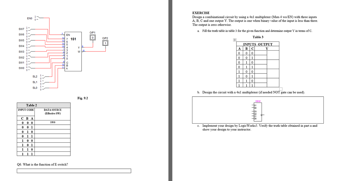
Transcribed Image Text:EXERCISE
Design a combinational circuit by using a 4x1 multiplexer (Mux-4 wo/EN) with three inputs
A, B, C and one output Y. The output is one when binary value of the input is less than three.
ENO
0-
The output is zero otherwise.
SW7
a. Fill the truth table in table 3 for the given function and determine output Y in terms of C.
O/P1
SW6
EN
Table 3
12
7 151
O/P2
SW5
13
6
14
5.
INPUTS OUTPUT
SW4
15
15.
4
Y
ABC
Y
SW3
w lke
1
Sw2
0 0 1
SW1
1
10
11
1 1
SWO
A
0-
1
1
SL2
1
0 1
1-
1
1
SL1
| 1
1
1
1
SLO
b. Design the circuit with a 4x1 multiplexer (if needed NOT gate can be used).
Fig. 9.2
DEV
Table 2
IS1
So
INPUT CODE
DATA SOURCE
D3
D2
D1
(Effective SW)
сВА
0 0 0
0 0 1
SwO
c. Implement your design by Logic Works5. Verify the truth table obtained in part a and
show your design to your instructor.
0 1 0
0 1 1
1 0 0
1 0 1
1 1 0
1 1 1
Q6. What is the function of E switch?
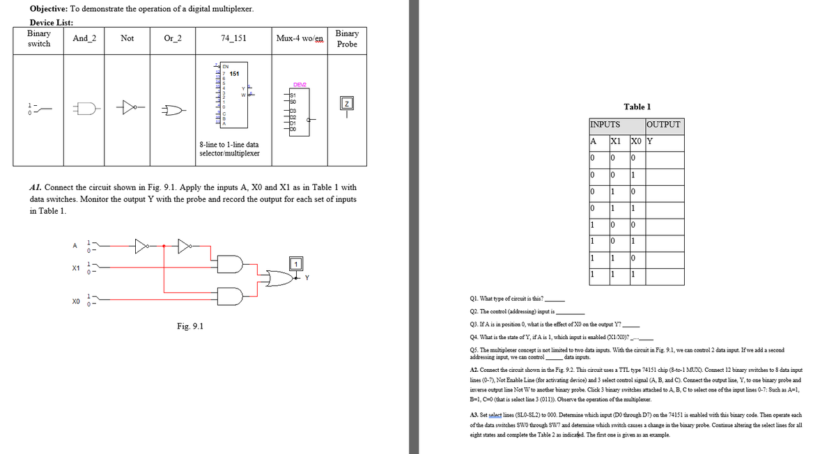
Transcribed Image Text:Objective: To demonstrate the operation of a digital multiplexer.
Device List:
Binary
switch
Binary
And 2
Not
Or_2
74_151
Mux-4 wo/en
Probe
EN
151
DEV2
Table 1
INPUTS
OUTPUT
A
X1
xo Y
8-line to 1-line data
selector/multiplexer
lo
lo
10
10
lo
1
A1. Connect the circuit shown in Fig. 9.1. Apply the inputs A, X0 and X1 as in Table 1 with
10
1
10
data switches. Monitor the output Y with the probe and record the output for each set of inputs
in Table 1.
1
1
1
0
lo
1
A
1
10
X1
1
1
Q1. What type of circuit is this?
Q2. The control (addressing) input is.
Fig. 9.1
Q3. If A is in position 0, what is the effect of X0 on the output Y?_
Q4. What is the state of Y, if A is 1, which input is enabled X1/X0)? ._
Q5. The multiplexer concept is not limited to two data imputs. With the circuit in Fig. 9.1, we can control 2 data input. If we add a second
addressing input, we can control
data inputs.
A2. Connect the circuit shown in the Fig. 9.2. This circuit uses a TTL type 74151 chip (8-to-1 MUX). Connect
binary switches to 8 data input
lines (0-7), Not Enable Line (for activating device) and 3 select control signal (A, B, and C). Connect the output line, Y, to one binary probe and
inverse output line Not W to another binary probe. Click 3 binary switches attached to A, B, C to select one of the input lines 0-7: Such as A=1,
B=1, C=0 (that is select line 3 (011)). Observe the operation of the multiplexer.
A3. Set select lines (SLO-SL2) to 000. Determine which input (DO through D7) on the 74151 is enabled with this binary code. Then operate each
of the data switches SW0 through SW7 and determine which switch causes a change in the binary probe. Continue altering the select lines for all
eight states and complete the Table 2 as indicated. The first one is given as an example.
Expert Solution
This question has been solved!
Explore an expertly crafted, step-by-step solution for a thorough understanding of key concepts.
Step by step
Solved in 2 steps

Recommended textbooks for you
Computer Networking: A Top-Down Approach (7th Edi…
Computer Engineering
ISBN:
9780133594140
Author:
James Kurose, Keith Ross
Publisher:
PEARSON

Computer Organization and Design MIPS Edition, Fi…
Computer Engineering
ISBN:
9780124077263
Author:
David A. Patterson, John L. Hennessy
Publisher:
Elsevier Science

Network+ Guide to Networks (MindTap Course List)
Computer Engineering
ISBN:
9781337569330
Author:
Jill West, Tamara Dean, Jean Andrews
Publisher:
Cengage Learning

Computer Networking: A Top-Down Approach (7th Edi…
Computer Engineering
ISBN:
9780133594140
Author:
James Kurose, Keith Ross
Publisher:
PEARSON

Computer Organization and Design MIPS Edition, Fi…
Computer Engineering
ISBN:
9780124077263
Author:
David A. Patterson, John L. Hennessy
Publisher:
Elsevier Science

Network+ Guide to Networks (MindTap Course List)
Computer Engineering
ISBN:
9781337569330
Author:
Jill West, Tamara Dean, Jean Andrews
Publisher:
Cengage Learning

Concepts of Database Management
Computer Engineering
ISBN:
9781337093422
Author:
Joy L. Starks, Philip J. Pratt, Mary Z. Last
Publisher:
Cengage Learning
Prelude to Programming
Computer Engineering
ISBN:
9780133750423
Author:
VENIT, Stewart
Publisher:
Pearson Education

Sc Business Data Communications and Networking, T…
Computer Engineering
ISBN:
9781119368830
Author:
FITZGERALD
Publisher:
WILEY