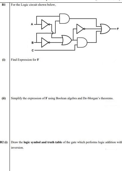
For the Logic circuit shown below, Find Expression for F


Q: Analyze the logic circuits shown below in order to obtain the logic function for each circuit. Write…
A:
Q: Design the logic circuit for asynchronous up counter that counts the number of students in a class…
A: According to the question, we need to design mode 25 asynchronous counter by using JK FF.
Q: a) Design a combinational logic circuit that reduces a 6-bit signed number by 5. Include overflow…
A: Consider the 6-bit signed number is given as: A5A4A3A2A1A0 The reduction in 6-bit signed number by 5…
Q: 18. Derive the Boolean expression for the logic circuit below: a. CA + CB +CD A B b. C(A + B)D с.…
A:
Q: Simplify the given expression to its SOP form. Draw the logic circuit for the simplified SOP…
A:
Q: Design a combinational Logic circuit in which whenever input is an even number between 1 and 10 a…
A: The logic circuit can be designed by using the truth table and the reduced Boolean expression can be…
Q: Given the function G=(A’+B+C)(A’+B’+C’)(A+B+C) Draw the logic circuit diagram of the simplified…
A:
Q: Draw the logic circuit of 3 bit comparator
A: A comparator is a combinational logic circuit that compared the orders of magnitude of two binary…
Q: Find the output expression of the logic circuit. F C
A: Given logic circuit,
Q: Given a combinational logic circuit whose input is a four-bit number and whose output is the 2's…
A: Combinational logic circuit- It is defined as a circuit which is formed by the combination of logic…
Q: JA JB Kg CLK
A: Here, the flip flop used are J-K flip flop. Write the truth table for J-K flip flop. Inputs…
Q: Q1. Determine the output waveform and Boolean expression X of the logic circuit in given circuit.
A: Given circuit Y1 is the output of bubbled OR gate Y1=A'+B' Y3 is the output of NAND gate Whose…
Q: * For the logic circuit shown below FA F F=AB O F=A'+B' O F=A+B O F=AB'+A'B O ABO
A: In this answer we will find the resultant expression of F as explained below.
Q: b) Develop the truth table for the combinational logic circuit shown below.
A: Given combinational logic circuit shown
Q: Redesign by using D flip-flops and give the state diagram for the logic circuit after the redesign.…
A:
Q: Design a logic circuit that takes a 4-bit Gray codeinput from an optical encoder and determines if…
A: The truth table of the logic circuit that takes a 4-bit Gray code and determines if the input value…
Q: BA
A:
Q: From the following kmap, design the combinational logic circuit using 4:1 mux
A: Given the truth table of the combinational circuit as shown below: We need to design combinational…
Q: if we want to design a logic * circuit that make selective complement for example, to complement the…
A: Here the properties of all the gates given in the options are analysed and find out the answer.
Q: 4. A combinational logic circuit that compares between two 2-bit numbers A (AI A0) and B (RI RO) is…
A:
Q: For the given Boolean function: F = ABC+ABD+A’BCD’+AB’C’+B’CD i) Find the minimal Sum of Product…
A:
Q: (a) Simplify the following Boolean expression 'A' and draw the logic diagram for the simplified…
A: In this answer we will try to simplify the given Boolean expression using different laws. We will…
Q: Minimize the following Equation by using Karnaugh Map, then draw the final Logic Circuit of the…
A:
Q: Write the Boolean expression from given logic circuit diagram and simplify the output. Please show…
A: The Boolean expression can be obtained by writing the expression across all the gates.
Q: Design a BCD to excess 3 combinational logic circuit. Derive its simplified POS expression for all…
A: Let ABCD be the BCD number and WXYZ be the excess-3 number for given BCD number. Where A is MSB bit…
Q: Given that a logic ecircuit has the following Boolean expression: F = (A + C)(AB + AC) Convert the…
A: The given Boolean expression is, F=A+CAB+AC
Q: Find the minimum expression for the output ofthe logic circuit.
A: output of NAND gate is =AB¯ output of XOR gate is =B⊕C output of NOR gate is=AB¯+B⊕C¯ so f can be…
Q: Find the minimum expression for the logicfunction at the output of the logic circuit.
A: Here it is shown that all are NOR gates, Where, A and B are the inputs to the first NOR gate. B and…
Q: 2. Design a logic circuit to produce an output F = 1 if and only if the input which is %3D…
A:
Q: a. Construct a Karnaugh map for the logic function F = A ¯ B C ¯ D ¯ +AB C ¯ D ¯ + A ¯ B C ¯ D +AB C…
A: The above function is given as K-map is given as
Q: Draw the logic circuit represented by the following expression. X= A+B[C+ D(B + C)]
A:
Q: Investigate the logic gate using other gates. (2) (3) (4)
A: The digital circuits can be combinational as well as sequential circuits. The combinational circuits…
Q: Draw the logic circuit represented by the following expression. X= A+ B[C+ D(B + C)]
A:
Q: Sketch a sequential circuit that will turn on only if the input sequence is in the form of 11011.…
A:
Q: For the logic circuit shown in the figure below, derive the Boolean expression of Y, simplify it,…
A: Boolea Expression for the given circuit is: Y = ((A'.B')'.B + B.C')' Simplifying it we may get =…
Q: Question 2 a) Ali has bought stopwatch but it able to count the timing from 1s until 13 s only.…
A: 2a) Given, Sequence of counting for stop watch is 1s to 13s only. Counter design using JK…
Q: Design a hazard-free combinational logic circuit to implement the following logic function: f(a, b,…
A: In a combinational circuit, because of the transition of one of the inputs, if the output…
Q: Write the function implemented by the logic circuit given below.
A:
Q: Q2 /Answer the following questions Q2/A/ Implement the logic circuit that has the expression below…
A:
Q: Find the boolean expression for the logic circuit shown below.
A: The given logic circuit is shown below:
Q: Draw the given logic circuit using only NAND gates and write its output expression. B ÅÅ
A:
Q: design logic circuit of MODE 6 counter that count {7 3 1 5 3 0} use JK flip flop in your design?
A:
Q: utes remaining 20 Complete the truth table for the logic diagram shown that uses a multiplexer.
A: In this question, Find the truth table of the 8×1 MUX. Here A, B, C are selection lines
Q: AV Find the Boolean expression and the tratk tane for the X y z 'w logic design ?
A:
Q: For the logic diagram provided, give the logic expression for the output F. 35ns 25ns 5ns 25ns F-(…
A: Given the circuit diagram: We need to find the logic expression for the output F.
Q: in this exercise you are going to design and build two circuits to give the sum and carry unctions…
A:
Q: An IC 74S04 is belong to Schottky TTL logic family. Select one: OTrue False
A: Choose the correct option An IC 74S04 is belong to schottky TTL logic family as per our guidelines…

Step by step
Solved in 4 steps with 2 images


- Which of the following statements accurately represents the best method of logic circuit simplification? a. Actual circuit trial and error evaluation and waveform analysis b. Boolean algebra and actual circuit trial and error evaluation c. Karnaugh mapping and circuit waveform analysis d. Karnaugh mapping and Boolean algebraBook used is Digital Logic with Verilog Design by Brown & Vranesic. Study the counting circuit diagram below and answer the following questions: a. Based on the circuit drawing, is the Clock Positive-Edge Triggered or Negative-Edge Triggered? b. How was this determination made? c. What are the minimum and maximum valkues of the circuit? Explain. d. There are 3 grayed out boxes we refer to this symbolic use as _____________. Why are these used in circuit design?(1) Find out the logic expression of output Q for the circuit on the left. And prove this is equivalent to the D latch circuit on the right. (2) Explain which is better and why?
- Design a 4-bit arithmetic circuit, with two selection variables S1 and S0, that generates the arithmetic operations in the following table. Draw the logic diagram for a single bit stage. Note that B’ represents “Not B”. Draw the logic diagram for a single bit stagsimplify the logic circuit found in the figure below and provide the following: 1. Unsimplified Logic Expression 2. Simplification Process using Boolean Algebra 3. Simplified Logic Expression 4. Truth Table of the Simplified Logic Expression 5. Simplified Logic CircuitA combinational logic circuit that compares between two 2-bit numbers A (A1 A0) and B(B1 B0) is designed. Output F is high when ? > ? and low when ? < ?. 1) Are there any undefined outputs? If there are any undefined outputs what are the inputs?
- 1. Given the Boolean expression (b + d)(a’+ b’ + c),a. Convert the expression to the other standard form. What do you call this standard form?b. Derive its canonical form. What do you call this canonical form?c. Derive the other canonical form. What do you call this canonical form?d. Provide the truth table of the expressione. Draw the logic circuit diagrams of the 2 standard forms1) Design the logic gates that compare (3) bit binary numbers that are "equal" or "not equal." A0 B0 A1 B1 A2 B2 2) Derive the logic equations for both outputs 3) What type of circuit/system can this be used in an application you could create?4.1 Investigate if the following Boolean “identity” is correct, or not. If it is not correct, formulate the correct version of the identity (?′?+?)′=?+?′?′. [2]4.2 Use the identities of Boolean algebra to verify the following identity: [4]?(?+?)+??′+??′+?=?+?+?4.3 Consider the logic gate circuit below:a) Formulate the Boolean expression corresponding to the output of the logic circuit diagram above. [2]b) Hence, show that the Boolean expression formulated in part (a) reduces to ??+?. [3]c) Draw the logic gate circuit diagram corresponding to the reduced expression inpart (b) above. 3.1 Let r, s, t denote the statements “Joe is registered for MCI511S”, “Joe will go to the zoo next week”, “Joe is registered for PBT512S”, respectively. Translate the symbolic statement (∼?∨?)→∼? into words. [2]3.2 Write the negation of the statement “If Joe writes the exam, he will go the airport but he will not catch the flight”. [2]3.3 Determine the truth value of the compound statement (?∧∼?)∨∼?, if p…
- Using the analysis technique where you first extract the truth table and then use it to derive the output’s logic expression, analyze the circuit. Record your results below. I added the circuit as an image Conclusion In your own words, describe the process used to analyze a logic circuit where you first extract a truth table and then derive the logic expression. 2.Again, in your own words, describe the process used to analyze a logic circuit where you first extract the logic expression and then derive the truth table.Determine the simplified Sum of Product expression of Q1 and Q2 from the table using a K-Map, then draw the simplified logic diagram. SHOW KMAP WITH THE FINAL EXPRESSION & LOGIC DIAGRAMi) Analyze the logic circuit in Figure Q5(c) and obtain the Boolean expressionfor Z.ii) Construct a truth table from the logic circuit in Figure Q5(c) and explain it.