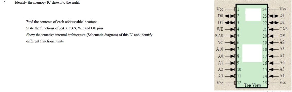
Identify the memory IC shown to the right: Vce 24 Vss DO 23 D3 Find the contents of each addressable locations D1 22 D2 State the functions of RAS, CAS, WE and OE pins 210 CAS 20 OE 19 A9 WE Show the tentative internal architecture (Schematic diagram) of this IC and identify RAS different functional units NC 18 AS 17 A7 16 A6 15 AS A10 A0 Al 9 A2 A3 11 14 A4 13 Vce 12 Vss Top View
Q: -) LDI R13 , 0x20 ) Harvard architecture consist of separate memories. ) MOV Cs, AX -) MOV AL, [BX]…
A: Step by step explanation is in given below.
Q: 5. How many AND gates are required to realize Y CD+EF+G? А. 4 В. 5 С. 3 D. 2 6. The Instruction…
A: Note: “Since you have posted a question with multiple sub-parts, we will solve three subparts…
Q: Consider the architecture as shown and the following instruction: link a6, #-8 Internal bus CONTROL…
A: Solutions !!
Q: Q4./DS 2000, SS 3000, BX-012A, BP-021B, DI 0010 SI 0020. 1. Compute the offset of each of the…
A: We solve the question in figure: Figure 1:
Q: Let the base addresses for I/O devices mentioned in (a) are 240, 244, 250, and 2F8 respectively.…
A: Required : Commands to load given address to devices
Q: Single-cycle MIPS Architecture 1. Assume that core components of single-cycle processor (shown…
A: Below is then answer to above question. I hope this will be helpful for you...
Q: Compute
A: RAM chip size =256 × 8 Required memory size= 2 k bytes = 2…
Q: Computer architecture True or false Please INeed Answer after 30 minutes 1_In UMA of MIMD system,…
A: Answer 1. UMA (Uniform Memory Access) framework is a common memory design for the multiprocessors.…
Q: chips (see below) plus a decoder, construct the block diagram of a 16M × 16 RAM s
A: Using multiple 4M × 8 RAM chips (see below) plus a decoder, construct theblock diagram of a 16M ×…
Q: 3. If a ROM chip in some 8-bit microcomputer system starts wita an address of 97C0H while its end…
A: If a ROM chip in some 8-bit microcomputer system starts with an address of 9700Hwhil its end…
Q: Standard 68k microprocessor-based systems contains Microprocessor Unit (MPU), Input Port with…
A: Within the microprocessor, It is written in assembly language. Programming in assembly language…
Q: Question 5 With reference to 8086 Microprocessors Pin Assignment: a) State the three groups of…
A: “Since you have posted a question with multiple sub-parts, we will solve first three subparts for…
Q: In order for the MARIE architecture to accommodate 2 ACs, 1. does the instruction (4 bit opcode…
A: 1. No, the instruction does not need to change. The MARIE architecture can accommodate two ACs by…
Q: 2. The 8-bit registers AR, BR, CR, and DR initially have the following values: AR= 11010010, BR=…
A: Actually, AR,BR,CR and DR are registers. The 8-bit registers AR, BR, CR, and DR initially have the…
Q: B) Let the base addresses for I/O devices mentioned in (a) are 240, 244, 250 and 2F8 respectively.…
A: Solve only Part B(a) Draw a block diagram of a microprocessor based system interfaced with 8255,…
Q: Q#03) (a) Explain and demonstrate the use of the RISC and CISC architectures in computer…
A: Given: Q#03) (a) Explain and demonstrate the use of the RISC and CISC architectures in computer…
Q: explain your answers In order for the MARIE architecture to accommodate 2 ACS, 1. does the…
A: 1.No, the instruction does not need to change. The MARIE architecture can accommodate two ACs by…
Q: Please answer both questions a)There are 3 forms of Program Memory Addressing Modes: Direct,…
A: The JMP instructions are used to jump to an instruction at an address given. a) CS is the code…
Q: Occasionally serial interfaces will have a FIFO instead of just the double-buffered architecture we…
A: Introduction: Serial Interfacing: Serial interfacing means we send one bit at time. Serial ports…
Q: What would be the clock period of a pipelined MIPS architecture with two stages, one comprising…
A: What would be the clock period of a pipelined MIPS architecture with two stages, one comprising…
Q: A microprocessor scans the status of an output I/O device every 20 ms. This is accom- plished by…
A: Introduction: In this question, we are asked to calculate the time to scan and service the device in…
Q: Evaluate the expression: F = (c -a)*d +e-b focusing 1- address through 3-address format. Also…
A: Solution Expression:- F = (c-a)*d+e-b USING 1-ADDRESS INSTRUCTIONS - LOAD c SUB a STORE R1 LOAD d…
Q: esign the hardware required to interface 64KB of SRAM to the demulti Idress and data bus of the 8086…
A:
Q: A computer employs RAM chips of 512 x 8 and ROM chips of 256 x 8. The computer system needs 1K…
A: Solution a. How many RAM and ROM chips are needed? Size of RAM Chip computer employs RAM chips=256x8…
Q: Q4) Suppose that DS-1020H, SS-2010H, BX-0300H, BP-1010H, and DI= 1100H. Determine the memory address…
A: Given that, DS=1020H SS=2010H BX=0300H BP=1010H and DI=1100H Given Instructions are:MOV [DI+300], AL…
Q: The 8-bit registers AR, BR, CR, and DR initially have the following values: AR= 11010010, BR=…
A: Given data The 8-bit registers AR, BR, CR, and DR initially have the following values:AR= 11010010,…
Q: Using multiple 4M × 8 RAM chips (see below) plus a decoder, construct the block diagram of a 16M ×…
A: Solution: Given, Using multiple 4M × 8 RAM chips (see below) plus a decoder, construct theblock…
Q: Example 2: Define machine cycle, describe the contents of the address, data and control bus lines…
A: given data
Q: Column X 1. MOV A, #25H 2. MOV R6, A 3. MOV 56H, A 4. MOV @RO, A 5. MOVC A, @A+DPTR Column Y A.…
A:
Q: The main reason a single-cycle processor datapath as taught in lectures must have separate…
A: Please find the answer below :
Q: QUESTION 1 A 4K×4 DRAM uses the following pins for addressing: O 6 address pins (AO-A5) and RAS and…
A: As per our guideline we must answer only first 3 questions for the MCQ's. Below are the answers with…
Q: Q5) The contents of a four-bit register is initially 1101. The register is shifted six times to the…
A: 5. The register is given the serial input with the serial data 101101. First digit from the left is…
Q: 1a. What are the operand types used in MIPS ISA. Explain each in your own words and give one example…
A: Operand types used in MIPS ISA: Memory: This consists of a register which has base address and an…
Q: For a 512k x 32 memory system, how wide does the incoming address bus needed to be in order to…
A: Here is the explanation about the width of the address bus:
Q: questions. One bus cycle 57 St S4 S7 CLK ADi-Aaa AS LDS UDS BAW DTACK from memory Chata memony…
A: Timing diagram of read cycle is given and after observing the diagram answers are given below
Q: List and explain the different addressing modes and instruction formats used in SIC/XE architecture.
A: Each format has a different representation in memory: Format 1: Consists of 8 bits of allocated…
Q: A decoder 74LS138 is to interface with 8086 microprocessor and a memory for perfect communication.…
A: Truth table design with perfect configuration:
Q: In the diagram
A: In the diagram, whose memory address ranges are not represented by chips 1 and 2? The address lines…
Q: 6) A DMA controller transfers 32 bit words to memory using cycle stealing. The words are assembled…
A: SUMMARY: -Hence, CPU will slow down by 0.6%.
Q: Consider the architecture as shown and the following instruction: link a6, #-8 Internal bus CONTROL…
A: Solution !!
Q: For the below microprogrammed architecture, what is the ALU sequence of actions/micro instruction…
A: Solution:-- 1)The given question is an type of the multiple choice question so some of the options…
Q: A computer employs RAM chips of 512 x 8 and ROM chips of 256 x 8. The computer system needs 1K bytes…
A: According to the question. A computer employs RAM chips of 512 x 8 and ROM chips of 256 x 8. The…
Q: QUESTION#3 Interface 8-bit input port (74LS245) to read the status of switches SW1 to SWB to the…
A: It is defined as the central unit of a computer system that performs arithmetic and logic…
Q: Q1.1 lw instruction execution. 4 Points With the given MIPS single-cycle CPU schematic, when Iw $8,…
A: We have MIPS Single Cycle Schemetic lw $8 4($9) lw = loads a word into a register $8 = temprary…
Q: Draw a block diagram of a microprocessor based system interfaced with 8255, 8254, 8259, 8237and…
A: In above question we make a microprocessor diagram which one have 4 ,8255 ,8254,8259,8237 and RAM.…
Q: Answer B part only! a) Draw a block diagram of a microprocessor based system interfaced with 8255,…
A: Question:
Q: A- implement 32KX 16 EPROM using 8K*8 EPROM Ic's and 2:4 decoder? B- Design microprocessor 8086…
A: A. Total number of 8Kx8 chips required = 32Kx16 / 8Kx8 = 4*2 = 8 These 8 chips are arranged as 4…
Q: Q1/ Chose by True or False from The Following Sentences 1- The DMA module must use the bus only when…
A: 1. When DMA method is used for transferring large amount of data , it is more efficient. If we want…
Q: Draw a block diagram of a microprocessor based system interfaced with 8255, 8254, 8259, 8237 and…
A: 8255 Pin Diagram: Fig shows the 8255 Pin Diagram of Microprocessor. 8255 Block Diagram: Fig.…
Step by step
Solved in 2 steps with 2 images
- If a microprocessor has a cycle time of 0.5 nanoseconds, what’s the processor clock rate? If the fetch cycle is 40% of the processor cycle time, what memory access speed is required to implement load operations with zero wait states and load operations with two wait states?Draw a block diagram of a microprocessor based system interfaced with 8255, 8254, 8259, 8237 and RAM. Also show clock generator, buffers, transceivers and address decoder in the diagram: use 8086 in maximum mode Please helpComputer Science Occasionally serial interfaces will have a FIFO instead of just the double-buffered architecturewe described. Are overrun errors still an issue in those FIFO-based architectures? Why or why not?
- Solve only Part B(a) Draw a block diagram of a microprocessor-based system interfaced with 8255, 8254, 8259, 8237and RAM. Also show clock generator, buffers, transceivers, and address decoder in the diagram:use 8088 in minimum mode B) Let the base addresses for I/O devices mentioned in (a) are 240, 244, 250, and 2F8 respectively. Write assembly commands to load these control/command words in these devices.Q1:Suppose the initial physical address of a segment register is given by 0E41:A02EH. Determine the physical address, base and final address of that segment register of 8086 microprocessorQ#03) (a) Explain and demonstrate the use of the RISC and CISC architectures in computer applications, as well as their benefits and drawbacks in various applications, and write down their advantages and shortcomings in points. Assembler language codes for basic memory locations and addressing operations, together with timing diagrams, should be written down.
- Draw a block diagram of a microprocessor-based system interfaced with 8255, 8254, 8259, 8237, and RAM. Also show clock generator, buffers, transceivers and address decoder in the diagram:use 8088 in minimum mode.Identify if possible the type of addressing modes for the followinginstructions. 1. MOV [EBX + EDI + ABCDH], EDXQ: Show how a 64 Kbyte memory (32 Kbyte SRAM & 32 Kbyte EEPROM) Draw the complete schematic of the design indicating the address map. Assume the starting address of the EEPROM is 90000H and for SRAM 80000H. (Using any method you prefer).
- The 8051 serial port supports full duplex operation, with transmit and receive buffersthat are available via the SBUF register. Each buffer has an interrupt flag, symbolisedas TI and RI, respectively.i) Briefly state what is meant by full duplex communication. ii) Write a small assembly language program to show how the serial interface can beused for the reception of characters using the serial interface interrupt. Thereceived character(s) should be copied into R0. You must show how theinterrupt is configured; however, you can omit all details of the timer setup. iii) Assuming this code is run on a classic 8051 using a 16 MHz crystal, show howyou would configure Timer 1 for a baud rate 9600 bits/sec and calculate theresulting percentage error. Assume the serial interface is set for 8-bit UART mode,the SCON bit is 0, and the timer is to operate in 8-bit auto-reload mode. You mustshow the values of SCON, TCON, TMOD and TH1.a.) In the computer system, the Bus is said to be a collection of wires through which datais transmitted. The bus could be unidirectional or bidirectional depending on what isbeing done at a time. With reference to the type of buses explain this phenomena orprinciple. b.) How does the size or width of a Bus affect or influence the architecture of a computersystem with regards to data transmission? Explain with examples. c.) Explain the purpose of the Registers and Flags in the operation of the CPUREAL MODE MEMORY ADDRESSING 1. In the real mode, show the starting and ending address of the segment located by the following segment register values (in hex): a) SR= DC28b) SR=FA91 2. Find the memory location addressed by the microprocessor, when operated in the real mode, for the following segment register and 80286 register combinations: a) DS=8EBC & DX=A3D7b) CS=DCAF & IP=FAC8