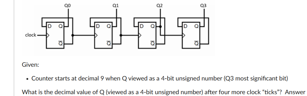
Q0 Q1 Q2 Q3 clock - Given: • Counter starts at decimal 9 when Q viewed as a 4-bit unsigned number (Q3 most significant bit) What is the decimal value of Q (viewed as a 4-bit unsigned number) after four more clock “ticks"? Answer


Q: Construct the circuit as shown below. Apply the 4-bit BCD digits through four switches and observe…
A:
Q: Draw a flow diagram for a 2-bit binary counter/clock that counts from 0 to 3 in decimal system using…
A: The counter is used to count by advancing the count of the counter with respect to each clock pulse,…
Q: Q2/ a- Draw completely the BCD Decoder Driver (7442) IC with 7- segment display b- What is the type…
A: According to the question,
Q: Design a code converter that converts a decimal digit from BCD to excess-3 code, the input variables…
A:
Q: For the circuit shown, a closed switch is represented by a logic 1, and an open switch by a logic 0.…
A: series switches are are named as a AND Gate. Parallel switches are called as OR gate. W and X…
Q: Fill in the values of the Carry, Sign, Zero and Overflow flags after each instruction has executed…
A: According to the question, we need to determine the condition of the flags after the execution of…
Q: You are given the following assembly language statements: MOV AX, 15225 MOV BL, 126 DIV BL SUB…
A: instruction MOV AX, 15225H: 15225H is moved to AX register MOV BL,126H: 126H is moved…
Q: Assume that memory location $c100 holds a data byte =$37, [ACCA]= $B8 and [ACCB]=$FE. For each of…
A: Given data: $37 data at memory location $C100ACCA=$B8ACCB=$FE
Q: 20. In Figure 5, How many clock pulses are required to add two, 4 bit binary number ? Register B…
A: The given circuit diagram is
Q: sll t2, t0, 6 or t2, t2, t1
A: The answer to the above problem is given below:-
Q: Q3: The content of a four-bit register is initially the 4-bit word 0000. The register is shifted…
A: Given Serial input serial output ,four bit register initial value of 0000 The serial input is given…
Q: The numbers from 0-9 and a no characters is the Basic 1 digit seven segment display * .can show…
A: 1.) Seven segment display consists of seven LED's. It is capable of display single digit number. It…
Q: c. Build the math mo D. Draw the logic ci
A: The digital boolean expression can be solved by different postulates such as distribution law,…
Q: "What is the result of executing the following instruction sequence? MOV DX, 2364H MOV BX, 1234H MOV…
A:
Q: After executing MOV AX,-11011 SAHF JNC WAQIQI (a) Will the processor jump? (b) repeat the solution…
A: MOV AX, -11011 SAHF JNC WAQIQI (a) will the processor jump after executing this (b) repeat the…
Q: Show the program execution for the following program. The hypothetical machine has four (4) opcodes:…
A: Show the program execution for the following program.The hypothetical machine has four (4)…
Q: Convert the binary NUMBER 10111110010.11010 to decimal number (Show the steps in paper, scan and…
A: We will multiply 20, 21, 22.....to the binary digit from left side of decimal point and right side…
Q: Please enter all answers in decimal. Consider the two 6-bit numbers x1 = 101101 and x2 = 111100.…
A: Considering the two 6-bit numbers x1=101101 and x2=111100. 1. We need to find the decimal equivalent…
Q: How to store (1050000)10 in register $s0? Write down the instructions that stores the data in $s0…
A:
Q: If a 10-bit ring counter has an initial state 1101000000, what is the state after the second clock…
A:
Q: Assume that memory location $c100 holds a data byte =$37, [ACCA]= $B8 and [ACCB]=$FE. For each of…
A: Note: As per our policy, I have attempted the first three subquestions. Given data: $37 data byte at…
Q: What is the Boolean expression corresponding to the shown digital circuits? A B OF= A(B+C) F= ABC' O…
A:
Q: Question 23 For the given values of D, Id, and clk, indicate the 3-bit load register's Q output…
A: As per our guidelines we are supposed to answer only first question. Kindly repost the other parts…
Q: a) Write the truth table and logical expression for a two-input EX-OR gate. b) Draw the IC pin…
A:
Q: Problem_#08] For the 4-bit parity generator shown, determine the output. It this circuit generating…
A:
Q: Here is the data flow diagram for a particular instruction. The various values shown indicate the…
A: For the given data flow diagram, instruction in binary is
Q: 9. The initial value of AX is 01011100, what will be the value of AX after the instruction NOT AX?…
A: In this question, We need to choose the correct options What is value kr AX after NOT AX…
Q: is the data flow diagram for a particular Instruction. The various Values shown Indicate the state…
A: Instruction in binary is as shown below
Q: (b) Using a synchronous binary counter as shown in Figure Q2(b), design and draw a counter to…
A: The synchronous counter is a electronic circuit which is based on binary logic of signals. This is…
Q: +Vc Q2 Q3 D CLK CUK K K K K CLK-
A: In the above circuit, we can see that the clock pulse is synchronized (i.e a common clock pulse is…
Q: The player controls in a particular video game are represented by numbers. The controls and their…
A: To solve above problem one should know how to convert a given binary number into decimal number. In…
Q: Design
A:
Q: Identify what type of Finite State Machine would be required to implement the given sequence: w =…
A: If output depends on present state as well input to the system then melay machine will be used If…
Q: A microprocessor that performs subtraction with complementary arithmetic; What value does the result…
A: A microprocessor that performs subtraction with complementary arithmetic;What value does the result…
Q: Q3=100011 solve Q3 O Q3=010110 Q3=110011 Q3/Assume that the microprocessor can directly address 64K…
A: We need 4 memory of 8k * 8 for 16k * 16 , We need to find out address for 4 memory .
Q: In a 4-bit ripple up-counter how many clock pulses will you apply, starting from state 0 0 0 0, so…
A:
Q: help
A: Given that,
Q: Q1- Design a binary multiplier that multiplies two 8-bit binary number by following design rules…
A: Given: The Q and B are the two separate 8-bit binary inputs, C is the 3-bit sequence counter and R…
Q: Design a code converter that converts a decimal digit from BCD to excess-3 code, the input variables…
A: The Code Converter is a tool for converting one binary code to another. Binary codes come in a…
Q: 3) Show how two 4:1 and one 2:1 mux could be connected to form an 8:1 mux. 4) Given the multiplexer…
A: As per our company's guideline we should solve only one question so please repost another question…
Q: 1. Assume that the registers are 8-bit wide. Consider the following code: MOV R1, #4A MOV R2, #40…
A:
Q: What is the value for the 32-bit register EAX after executing the mnemonic opcode/operand…
A: What is the value for the 32-bit register EAX after executing the mnemonic opcode/operand…
Q: Design a logic diagram to display a digit 5 using 7-segment display.
A:
Q: (B)- Choose the correct answer for the following questions (Choose FIVE Only) 1. Assume AL register…
A: Microprocessor: It is a central unit of a computer system which can do arithmetic and logic…
Q: Explain the following 68000 assembly program using flowchart. A8, B8, and R8 are three 8-bit…
A: Mealy model: Output depends on input and present state.
Q: What is the content of register $t1 after executing the instruction: SLL $t1,$t1,8 if its initial…
A: suppose $t1 is 0000 0000 0000 0000 0000 0000 0000 0000 0000 0000 0000 0000 0000 0000 1010 1010 Shift…
Q: The contents of a four bit register are initially 1011.The register is shifted six times to the…
A: Shift register is used to store multiple bits of data using group of flip flops. By using the clock…
Q: Draw the diagram of a SISO four-bit register. Assume that the content of the four-bit register is…
A:
Q: 1. Numbers, Codes, Logic, Circuits a) Convert 101001012 to decimal. b) Convert -6310 to binary using…
A: The solution is given below
Q: 10. Perform five bit (including sign), two's complement binary addition of the following decimal…
A:

Step by step
Solved in 4 steps with 1 images


- Perform the indicated arithmetic on the following signed 2’s complement binary numbers. a) 01011011 + 11100101 b) 01001 - 01110 c) 1111 + 1100 Note: The answer should show the 2’s complement binary result; also indicate if each result is positive or negative or overflowed (by writing “positive”, “negative” or “overflow” next to the binary answer) and then follow with the decimal value of the result if there was no overflow. Do not extend (add any additional length) to these representations, but rather use a binary number word size equal to those found in each problem statement.A digital circuit whose number of inputs is 3, how many possible combinations of inputs will it have?How to build this circuit? (on Digital or Logisim) Binary-coded decimal is an alternative method of representing integers using binary. In it, each base-10 digit is represented by four bits, thus each nibble takes one of 10 values (0000 through 1001). Therefore, using BCD, 42 (decimal) is represented as 0100 0010 (binary) and 196 (decimal) is represented as 0001 1001 0110 (binary). Create a circuit in Logisim that accepts as input a pair of two-digit integers represented as BCD and outputs their sum in BCD. Any and all Digital components are fair game. You can assume that all inputs will be valid BCD-encoded numbers.
- so we were asked to implement a 3-bit BCD number on DE0’s board segment display for quartus... using 7447 but 7447 has 4 inputs? (see attached screenshot for problem) also not sure what the items in the second screenshot should be doing? like i can put inputs and outputs..but i don't know what they are? and its not discussed other than they can supply power?Please answer this question in 10 mins i will surely rate your answer. 1. A combinational circuit adds either a 1 or 2 to a 4-bit binary number A. Assume that the inputs bb A3, A2, A1, A0 represent the 4-bit binary number. Another input is a control signal C. The circuit has outputs assumed to be X3, X2, X1 and Xo, which represent the 4-bit number X. When C=0, X=A+1 and when C=1, X=A+2. Assume that the inputs for which X > (1111)2 will never occur. Show the design steps in detail including truth tables, K-Maps, logic equation minimisation. Finally, design this circuit using only NAND gates and inverters .Using a single 7400 IC, construct a circuit to output the following Boolean function: F = A B + C D
- Act 1 problem solving this is a logic circuits and design laboratory subject please help me with this and screenshot all the solution and answers 2. What is the largest binary number that can be expressed with 16 bits? What are the equivalent decimal and hexadecimal numbers? Answer: 16 bits = ________= _______10 = ______16 3. Represent the decimal number 6,248 in: (a) BCD = (b) excess‐3 code = (c) 2421 code =Course: Computer Engineering Subject: Logic Circuit and Switch Theory Find a function to detect an error in the representation of a decimal digit in BCD. In other words, write an equation with value 1 when the inputs are any one of the six unused bit combinations in the BCD code, and value 0 otherwise. Course: Computer Engineering Subject: Logic Circuit and Switch TheorySubject Digital Logic Design(DLD) Design the truth table for Full Subtractor Circuit. Write the Boolean expression for Difference andBorrow. Also Draw the circuit diagram for Difference and Borrow.
- This question contains info on Digital Systems Logic Design and requires: Truth Table, KMapping and the Logic Circuits Designs. SEND the accurate answers labelled please.This Question is from Digital Logic Design Q1. Assume your register number EF20BCE014 is in Hexadecimal, where 014 are the three digits of your registration number. a) Represent your registration number in the binary. b) Split the ten digits of your registration into two Hexadecimal numbers M and N, where the left most five digits make number M and the right most five digits make number N. Using r’s complement, subtract N from M. In other words, calculate M – N.Design a circuit called half adder (HA) which adds two 1-bit numbers, a,b and produces 2-bit output, c. a. Draw the truth table of the circuit.b. Find the Boolean functions of each bit of the output.c. Optimize the Boolean functions.d. Draw the logic diagram of the optimized circuits.e. Write the VHDL code of the logic diagrams by using “Dataflow modeling” method f. Simulate the circuits that you have designed in 1.e. Prepare a simulation waveform for you report.g. Produce the RTL schematic for the circuit that you have designed in 1.e.