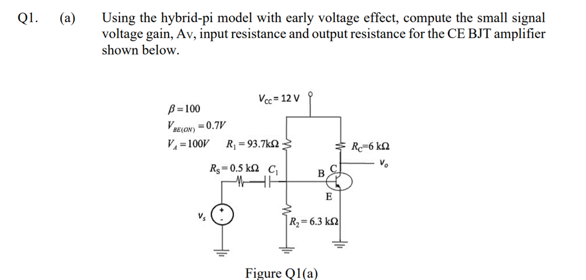
Q1. (a) Using the hybrid-pi model with early voltage effect, compute the small signal voltage gain, Av, input resistance and output resistance for the CE BJT amplifier shown below. Vcc = 12 V B=100 V BE(ON) = 0.7V V =100V R = 93.7k2 * R=6 kN Vo Rs= 0.5 k2 C E Vs R,= 6.3 kN


Q: (b) If the parameters for the BJT in Figure Q.1(b) are given as ß= 140, VBE = 0.7 V, VT=26 mV and…
A: For the above given common emitter amplifier circuit we need to calculate small signal hybrid π…
Q: Use a load-line analysis for the PMOS amplifier shown in Figure P11.24 to determine the maximum,…
A:
Q: Q3. R1= 400k , R2=400kN, R3=10kN, Vcc= 10V BJT parameters; B=150 , VBE = 0.7V Vcc R3 R13 c)…
A: R1 = 400k ohm R2 =400k ohm R3 = 10k ohm Vcc= 10V Beta = 150 VBE = 0.7 V Current Ic? VBE ?
Q: For the NPN amplifier circuit below, B221, VA5A V,0 point(0.19ma, 2.9V), R1-JOK ohm, R255K ohm,…
A:
Q: and its position may be established at any point along the load line by a suitable biasing…
A:
Q: A transistor amplifier which uses a npn BJT and various passive components is shown in figure Q1. A…
A:
Q: Sketch the AC load line for the amplifier circuit and fir the theoretical maximum symmetrical swing…
A: From given circuit maximum theoretical swing is…
Q: Figure 2 shows a BJT amplifier circuit. Given, V3 = 2.4 V and assume that the emitter current equals…
A:
Q: In Figure 3.3 shows the circuit diagram of a typical n-channel JFET common source amplifier. If ac…
A: The circuit parameter are given…
Q: Q1: a) What are the Q points for the transistors in the amplifier of the figure shown below? Assume:…
A: consider the given question;
Q: Consider the transisțor amplifier shown below where the coupling capacitors Ce1, Ca and the bypass…
A: Capacitor- capacitors are widely used in electronic circuits to block direct current power while…
Q: Activity 2: The amplifier circuit below has a single ac input and two ac outputs. Assuming…
A: Dear student as per our guidelines we are supposed to solve only one question in which it should…
Q: Consider the common-source amplifier shown in Figure P11.50. The NMOS transistor has KP=50 μA/V2,…
A:
Q: In the circuit below, we have two MOSFETS M1 and M2 with properties K1 and K2, respectively. Assume…
A: The circuit is as shown below,
Q: In a common emitter bjt amplifier circuit, what parameter is described by Bre. Choices: Diode…
A: In this question we will write about bjt hybrid model....
Q: 4/ Refer to the class AB power amplifier shown below: a. Determine the dc parameters VB(Q1), VB(Q2),…
A:
Q: Consider class-A emitter follower circuit shown in the figure below. The circuit parameters are V+ =…
A: The parameters of a Class-A emitter follower circuit are as follows,V+ =…
Q: Using approximate method, the DC operating parameters of the common emitter BJT amplifier are as…
A:
Q: a) Using the hybrid-pi model with early voltage effect, compute the small signal voltage gain, Av,…
A:
Q: Q1. Design a MOSFET current source circuit to meet a set of specifications: The circuit to be…
A: VG12,VG34 are constant so they are grounded. Rout=VTIT=gm2ro2ro4Rout=gm2ro2ro4…
Q: Explain in detail, effect of Early voltage in transistor. Determine the equivalent output…
A: PART (1) : When a BJT is biased in active region the base emitter junction is forward biased and the…
Q: 1. For the amplifier circuit shown, do the VDp = +1.8 V following: RG а. Sketch the small signal…
A:
Q: Draw the small-signal equivalent circuit of the complete amplifier and perform an ac analysis to…
A: Small-signal modeling of the amplifier
Q: (b) Figure Q2(b) shows a BJT amplifier with ß = 120 and VBE = 0.7 V. (i) Calculate current, IB, Ic…
A: Given: β=120 and VBE=0.7 V
Q: The amplifier circuit below has a single ac input and two ac outputs. Assuming transistor parameters…
A: Given: The amplifier circuit below has a single ac input and two ac outputs. Assuming…
Q: Design a two-stages amplifier circuit MOSFET-BJT (no bypass for the second BJT, all BJTs are in…
A:
Q: Using the hybrid-pi model with early voltage effect, compute the small signal voltage gain, Av,…
A: First we will do DC analysis to hybrid parameters then we will do ac analysis to calculate voltage…
Q: Question 4 Consider the common-collector BJT amplifier circuit in Figure 4. Assume that the…
A: We need to dc analysis and ac analysis to find out gain and input impedance .
Q: (a) What are the Q-points for the transistors in the amplifier as shown if VCC = 15 V, VEE = 15 V,…
A: given that, VCC = 15 V, VEE = 15 V, IEE = 400 μA, βF = 100, REE = 270 kΩ, RC =47 kΩ, VA=∞, and βF…
Q: A Class B amplifier, as shown in Figure QI(b), is operated at maximum power conversion efficiency.…
A: Part (i) It is given that the maximum power dissipation rated at 2 W but it can be operated not…
Q: 11 V- Vin || OV 60000 1500Ω 3300 100 Ω Vout
A: “Since you have posted a question with multiple sub-parts, we will solve first three subparts for…
Q: n the circuit shown in Figure 1, the input signal vsig is a small sine-wave signal with zero…
A: Steps for small signal analysis: 1. DC sources are considered as zeros i.e. voltage source are…
Q: In this circuit below, the Q₁, Q₂ operate in the active region. VDD = 10V, Rs = 15k№, RC1 = RC2 =…
A: Amplifier: Amplifier increases the current, power or voltage of a signal. this is a electronic…
Q: 6) Determine the following parameters according to power amplifier BJT circuit which is given below.…
A:
Q: Determine the values for the resistors R1, R2 and RE that would meet this requirement. Assume VBE =…
A:
Q: Summary: IOA The circuit in Figure 3 contains an ideal operational amplifier. (a) Use the "NVA-ish"…
A:
Q: H.W3: For a class B amplifier providing a 22-V peak signal to an 8- load and a power supply of…
A: Given a class B amplifier providing a 22-V peak signal to an 8 Ω load and Vcc=25 Vhere we have to…
Q: In the circuit below, the transistor has Ic = 1mA, IB = 5µA, and VBE = 0.5V. The source %3D current…
A:
Q: When BJTs are used in digital circuits they usually operate in the: a. active region b. breakdown…
A: In this question we will write about BJTs related questions....
Q: ut For the circuit above, Q₁ is in active mode and ignore early effect. Let Ic1=1mA, R=250ohm,…
A: The circuit diagram of the amplifier Circuit parameters are given as…
Q: QI. Using the hybrid-pi model with early voltage effect, compute the small signal voltage gain, Av,…
A: First we will do dc analysis and then we will do ac analysis to calculate gain and input and output…
Q: Enclosed please find an amplifier circuit designed with a BJT transistor. VCC = 9Volt for the…
A: DC analysis of the given system
Q: 01.) Suppose you had the BJT circuit below as part of a system that only operates correctly when the…
A: From the circuit shown question, the voltage at emitter terminal is 0 V and the BJT is a N-P-N…
Q: o1.) Suppose you had the BJT circuit below as part of a system that only operates correctly when the…
A:
Q: The parameters of the circuit shown Q1 are VDD = 5 V, R1 = 520 kN, R2 = 320 kN, RD = 10 kQ. Assume…
A:
Q: 1ΚΩ R₁ 22ΚΩ R₂ 2.7ΚΩ RE C3 220Ω Figure 1 Figure 1 is a BJT small signal amplifier circuit. Answer…
A:
Q: Q (i) Sketch a feasible class A silicon BJT Power Amplifier that provides a high voltage gain using…
A: As per our policy we can provide solution to first question only. As we have given : VCC=15 Vη=50…
Q: In the above circuit, BJT's VT values are not identical. a) For the collector currents of…
A: Note: We are authorized to answer three subparts at a time since you have not mentioned which part…
Q: Problem 4 V DD=+5 V MOSFET Parameters: Kn = Kp = 2 mA/V² |VTN| = |Vr| = 0.75 V Am = 2p = 0.01 Vi…
A: A) Here VSG1=VSG2=VSG...................1ID1=ID1=ID=IREF...................2 By current mirror…
Q: Use the following process parameters Tox =9.10"m, 4, = 350.10 "(m /V-S],Vr = 0.7V,7 0.45 For the…
A: It is given that: Tox=9×10⁻⁹ mμn=350×10-4 m2v-sVTo=0.7 Vγ=0.45…

Step by step
Solved in 2 steps with 1 images

- NFET Common Source Amplifier with Source Degeneration: For the circuit below, assume the MOSFET operates in saturation and is characterized by parameters V_TN and K_NThe transistor parameters for the NMOS common source amplifier given in the figure are VTN = 1.0V, kn = 0.8mA / V2 and alpha = 0. Circuit parameters are VDD = 10V, RS = 0.8k, RD = 3K, R1 = 210K and R2 = 140k. Find the IDQ drain current and VDSQ drain-source voltage at the transistor's Q - operating point. Determine in which region the transistor is operating.Vs=100 mV peak-to-peak, 1 kHz sine signal, Kn=0.4mA/v^2 ,Vt=1V , λ=0.01V^-1 Make the DC analysis of the above given mosfet amplifier circuit. Simulation to tableWrite down the measured values and mathematical calculation results. (The valueswith the units.)DC Parameters ,Measured value ,Calculated ValueVGETCVGSVDVDSIDb. Draw the small signal model for the AC analysis of the circuit. Find the gm, ro, Av values.c. Show the Vs input signal and the Vo output signal of the circuit on the oscilloscope. Volt/div of channels andSpecify time/div values.
- The given circuit is a 2N4403 PNP common collector amplifier. Let VCC=12V, VEE=-12V, R1=52.5kΩ, R2=33kΩ, and RE=2.5kΩ. Determine IB, IC, IE, VB, VC, and VE. Start by initially assuming |VBE| =0.7V or and assuming a value of beta (β). Where to look for the value of β? (Hint: It’s in the transistor model assigned). Determine the input voltage (may extend from the supply voltage range) where the BJT goes from “cut-off to active” and where it goes from “active to saturation”. Assume VCE=0.3V (edge of saturation), RL=500Ω, and C1, C2→∞.For the BJT amplifier circuit of figure below with the following parameters:β = hfe ≈ 250, re= 20.3Ω, and ro = 1/hoe ≈ ∞ Ω, Zb= 50.26KΩ determine:(a) Draw the Ac equivalent circuit in re- model and hybrid model.(b) hie, , Zi , and Zo'(c) Av using h- model.(d) Avs and ac output voltageThe small-signal resistance (i.e., dv/dlp) in kn offered by the n-channel MOSFET M shown in the figure below, at a bias point of V 2V is. (Device data for M: device transconductance parameter, = KN = H₂Cox () = 40, threshold voltage VTN = 1V, and neglect body effect and Lambda)
- Derive the expression for the following in terms ONLY of the small signalparameters and the given circuit components from the hybrid-pi model (Neglect the effect of the BJT’s small signal output resistancero):a.) RINb.) Gmc.) ROUTSuppose the tail current source is implemented using another transistor with the same BJT parameters, what would be the common-mode input range of this amplifier? Where V2>= VCM>=V1. Determine V1 and V2.a.) Consider a two-BJT configuration in Figure 1. You may assume that both transistors are the same with the same β, VBE,on = 0.7 V, and VCE,EOS = 0.3 V. Determine the minimum voltage VBE that will turn ON both Q1 and Q2. b.) Using the BJT small-signal model given in Figure 2, determine the AC current gain Ai = iout/iin for the circuit given in Figure 3. Assume ro >> rπ. You may assume that β is large.
- 5) Design a Common source E-MOSFET amplifier and write the formula of voltage gain.What type of bias circuit can be used for the BJT amplifiers? Can the same type of bias circuit be configured as different types of BJT amplifier? Briefly answer.In the circuit given in the figure, Vcc = 15 V, R1 = R2 = 10kΩ, RE = 1KΩ, RL = 0.5kΩ and transistor parameters are given as VBE = 0.7V, ßdc = ß0 = 100. a. Calculate the values of DC bias currents and voltages (IBQ, ICQ and VCEQ). b. Draw the small signal equivalent circuit of the circuit using the hybrid model of the transistor. c. Derive the input impedance expression of the circuit and calculate its value. d. Derive the AVI and AVG voltage gain expressions and calculate their values. e. Derive the current gain expression AI = I0 / Ii and calculate its value. Compare this value you have calculated with the value you will calculate using the expression Aİ = Zi AVI / RL.