Q4 (a) Figure Q4(a)(i) shows two unit of 74LS293 (4-bit binary counter) configured to generate multiple clock source. Referring to the internal circuit diagram of this IC shown in Figure Q4(a)(ii), obtain the frequency at fi, f2 and f3. f2 f3 f1 (10) CP 1 (8) (10) CP (8) 100HZ- Q4 (11) CP (4) (11) CP (4) Q2 Q2 (5) Q! Q1 (5) (12) MR, & (9) QO (12) MR, & (9) QO (13) MR (13) MR Figure Q4(a)(i) 2.
Q4 (a) Figure Q4(a)(i) shows two unit of 74LS293 (4-bit binary counter) configured to generate multiple clock source. Referring to the internal circuit diagram of this IC shown in Figure Q4(a)(ii), obtain the frequency at fi, f2 and f3. f2 f3 f1 (10) CP 1 (8) (10) CP (8) 100HZ- Q4 (11) CP (4) (11) CP (4) Q2 Q2 (5) Q! Q1 (5) (12) MR, & (9) QO (12) MR, & (9) QO (13) MR (13) MR Figure Q4(a)(i) 2.

Chapter22: Sequence Control
Section: Chapter Questions
Problem 6SQ: Draw a symbol for a solid-state logic element AND.

Related questions
Question
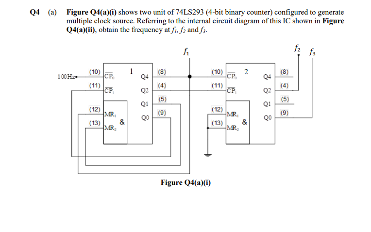
Transcribed Image Text:Q4 (a) Figure Q4(a)(i) shows two unit of 74LS293 (4-bit binary counter) configured to generate
multiple clock source. Referring to the internal circuit diagram of this IC shown in Figure
Q4(a)(ii), obtain the frequency at f1, f2 and f3.
f2
f1
f3
1
(10)
2
CP
(10)
(8)
(8)
100 Hz-
CP
Q4
Q4
(11)
CP
(4)
(11)
CP
(4)
Q2
Q2
(5)
(5)
Q1
Q!
(12)
MR,
&
(12)
MR
(9)
(9)
&
(13)
MR:
(13)
MR:
Figure Q4(a)(i)
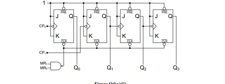
Transcribed Image Text:PRE
PRE
PRE
PRE
Q
Q
Q
J
CP.
K
K
K
K
CLR
CLR
CLR
CLR
CP;
MR,.
Qo
Q1
Q2
Q3
MR2
Expert Solution
This question has been solved!
Explore an expertly crafted, step-by-step solution for a thorough understanding of key concepts.

This is a popular solution!

Trending now
This is a popular solution!

Step by step
Solved in 2 steps with 2 images

Knowledge Booster


Learn more about
Need a deep-dive on the concept behind this application? Look no further. Learn more about this topic, electrical-engineering and related others by exploring similar questions and additional content below.Recommended textbooks for you