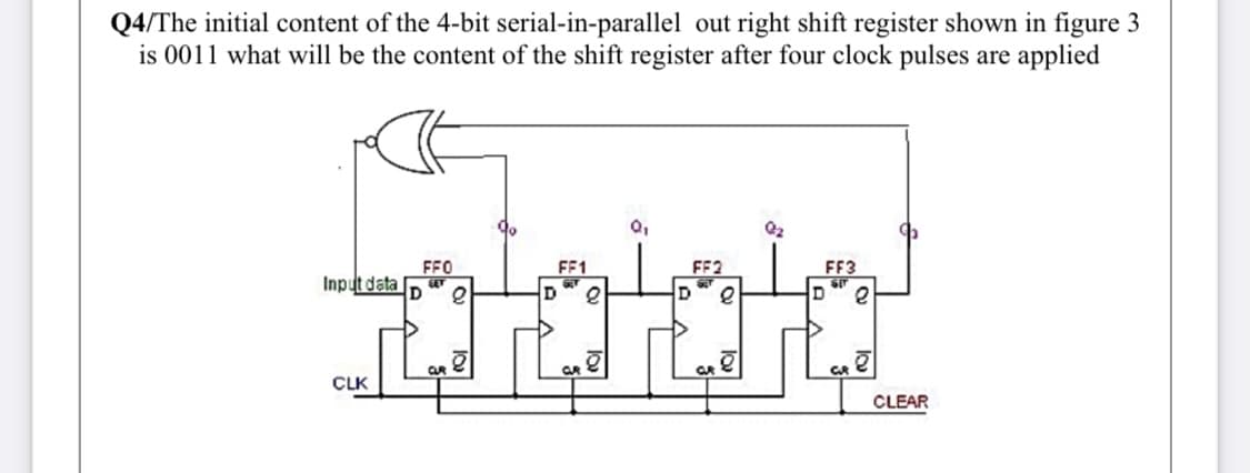
Q4/The initial content of the 4-bit serial-in-parallel out right shift register shown in figure 3 is 0011 what will be the content of the shift register after four clock pulses are applied Q2 FFO FF1 FF2 FF3 Input data D. CLK CLEAR


Q: Design a 3-bit shifter for the following operations: (i) (ii) (iii) No Shift Serial Left Shift by…
A: Since you have posted a question with multiple sub-parts, we will solve the first three sub-parts…
Q: Which data input line of the shift register must be tied LOW for the wait-state generator in figure…
A: The digital circuits can be sequential or combinational circuits. The combinational circuits depend…
Q: X is a 16 bit register and X-FEBAH. What is the result of the following operations in hexadecimal…
A: X is a 16 bit register and X=FEBAH . We need to find the result of the following operations: d. SHL…
Q: 2 Draw the state table and state graph for the follwineg logic Cirat X- TA A A To B cLK
A: The solution is given below
Q: 6.) The following waveforms are the input to the shift register you constructed in question #5.…
A: A good problem on digital electronics. Look below for solution:-
Q: How many shift pulses would be required to shift the contents of one six-stage register to another…
A: As per our company guidelines we are supposed to answer only first question kindly repost other…
Q: Write an instruction that stores a double-word value
A:
Q: Q2/ Choose five only 1-A stage in shift register consist of a) latch b) Flip flop c) Byte of storage…
A: As per the honor code I will do first three questions. Kindly repost the other questions again.…
Q: A 6-bit Flash ADC has - possible output codes. a. 63 b. 64 C. 6 d. 65 While using ARDUINO UNO to…
A: Analog to digital converter is used to convert an analog signal into a digital signal by using…
Q: 3. A microprocessor has .. . address bus b. bi-directional a. unidirectional c. Both 4. Instruction…
A: Length of Address Bus of 8085 microprocessor is 16 Bit (That is, Four Hexadecimal Digits), ranging…
Q: H.W:- 1) A four logic-signal A,B,C,D are being used to represent a 4-bit binary number with A as the…
A:
Q: The 4-bit multi-function register (Q) employed in the following logic circuit has two control inputs…
A: Given Four bit multi function register (Q) has a two control inputs (s0,s1)
Q: Select the statement which is not correct about Bus Interface Ur a. BIU is connected to the /O…
A: Bus interface unit This unit handles all transfer of data and addresses on the buses. This unit…
Q: Identify the type of register from the figure: Data in Do D, D2 D3 SHIFT|LOAD SRG 4 Serial data out…
A: In this we will write register type..
Q: Q2/ Choose five only 1-A stage in shift register consist of a) latch b) Flip flop c) Byte of storage…
A: We are authorized to answer three subparts at a time since you have not mentioned which part you are…
Q: Q In the arithmetic operations in ALU the meaning of arithmetic shift left instruction for a binary…
A:
Q: In class, we have seen the procedure for expressing decimal numbers in base 2 (binary), 8 (octal),…
A:
Q: The bit sequence 0100 is serially entered into a 4-bit parallel out shift register that is initially…
A: We are authorized to answer single question at a time since you have not mentioned which question…
Q: 1. Provide the outputs of Q3, Q2, Q1, and Q0 by completing the timing diagram of the…
A: Timing diagram: The timing diagram shows at what timing flip-flop works when the input signal is…
Q: 11. At TO the content of the register is 0000. What is the content of the register at T1? T4 T3 T2…
A:
Q: What is the output 'Q' of the given logic diagram? A- Da B - O*Q = Ã + B O b. Q = A.B O Q = A + B O…
A: From the NOR gate output
Q: Q2: A) What are the addressing mode and physical address for each instruction if you know .…
A: Given data for the Question is ES= A100H DS=4200H SS=D000H BX=0200H BP=1000H DI=0300H SI=0400H
Q: Assume that a digital system has eight 8-bit registers RO to R7. Assume that initially the register…
A:
Q: Q4/The initial content of the 4-bit serial-in-parallel out right shift register shown in figure 3 is…
A: In the question We are determine the content of the shift register after 4 cycle.. All are D flip…
Q: Q5: Fill in the following blanks with appropriate answers (Choose Five Only) 1. The instruction that…
A: 1) DEC 2) register 3) ADC
Q: Q4/The initial content of the 4-bit serial-in-parallel out right shift register shown in figure is…
A:
Q: Th mpute the physical address for the specified operand in each of the following instructions.…
A: As per our policy we can provide solution to first question only. As the given instruction is: MOV…
Q: The initial contents of the 4-bit serial-in-parallel-out shift register shown in the figure below is…
A:
Q: You have used DEBUG to unassemble the following instructions. -U 0100 0108 1369:0100 B84365 MOV AX,…
A: The instruction is loaded at location 0106, the instruction takes two bits when the given code is…
Q: 1. Construct a state diagram for the following sequence detector. The finite-state machine (FSM) has…
A: “Since you have asked multiple questions, we will solve the first question for you. If you want any…
Q: Q5/ The total clock that use to input and output data for 7-bit parallel in 3 parallel out shift…
A: Parallel-in parallel-out shift register: A parallel-in parallel-out shift register is a shift…
Q: Design 4-bits shift register with two control inputs A and B the register operate according to the
A: The design using is drawn below. Here apart from the D flip flops, 4 nos. 4 to 1 MUX has to be used…
Q: If the SHIFT/LOAD line is LOW, data a. is loaded from Do, D1, D2 and D3 immediately b. is loaded…
A: A simple problem on digital electronics . Look below for solutions:-
Q: Q: Compute the physical address for the specified operand in each of the following instructions. The…
A: "According to our guidelines, we can answer only three subparts at a time. Kindly, repost the…
Q: A register cell is to be designed with registers RO and R1 that has the following register…
A: According to the question, we need to design a circuit that performs the following operations
Q: Q4/The initial content of the 4-bit serial-in-parallel out right shift register shown in figure 3 is…
A:
Q: Q4/The initial content of the 4-bit serial-in-parallel out right shift register shown in figure 3 is…
A: In the circuit, Initial value 0011 Find the value after 4 cycle . We know D FF Output Q= D
Q: 2:STATUS Register has Individual Bits ndicate status of ALU operations ) 6 are status flags and 3…
A: In this question we will write about status and control flag for 8086 microprocessor...
Q: Suonortine.cxcentions &interruats Select True/False (T/F) for each statement. Exception usually…
A: According to the question, we need to determine the T/F statements as shown below
Q: Explain the process of the following Load D3 · D3 12 12 D2 Do Clock D Load Block Diogram of 4-bit…
A: Given
Q: The LC-3 ISA has been augmented with the following push and pop instructions. Push Rn pushes the…
A: According to the question, we need to calculate the value of a, b, c, d.
Q: 1. Shift registers can operate in both serial and parallel modes. List all four possible…
A:
Q: S. Set- R. Do 5 Qo Do . Reset- Q1. Qo
A:
Q: Q4/The initial content of the 4-bit serial-in-parallel out right shift register shown in figure is…
A: Initial value 0011 What will be content of the shift register after 4 clock . We know D flip flop…
Q: A microprocessor has an increment memory direct instruction, which adds 1 to the value in memory…
A: Total no. of cycles required in increment memory direct instruction:- fetch opcode:- 4 cycle fetch…
Q: Q. 3 For the following 4-bit shift register draw complete the timing diagram if the input (Data_in)…
A:
Q: : Design 4-bits shift register with two control inputs A and B the register operate according to the…
A: Given: The two control inputs A and B the register operate according to the following function…
Q: estion 1 A 5-bit serial input circulating shift right register shown below with initial value =…
A: In this question, Choose the correct option What is value of output after 4th cycle.
Q: Q2/ Choose five only 1-A stage in shift register consist of a) latch b) Flip flop c) Byte of storage…
A: 2. B Generally shift registers are made up of flip flop. Registers are used to store the data if we…
Q: is used to transfer a byte from an even address in the memory. O a. DO-D15 O b. DO-D7 O c. D8-D15 O…
A: Byte data with an even address (A0 is low) are transferred on the D7-D0 bus lines, Byte data with an…

Step by step
Solved in 2 steps


- The 3-bit shift register is shifted five times to the right with the serial input being 1011101. What is the content of the register? (Write your answer using only 0s and/or 1s.)Topic is about shift registers in electrical engineering. 1. What is the main functional purpose of a register? We are looking for the specifics of what a register does in isolation, not with respect to applications. 2. In what cases might we use serial and parallel inputs/outputs? 3. Describe the purpose of the debouncer in your own words. 4. Is an SN5474 the same as an SN 7474? If not, how do they differ?This Question is from Digital Logic Design Q1. Assume your register number EF20BCE039 is in Hexadecimal, where014 are the three digits of your registration number.a) Represent your registration number in the binary.b) Split the ten digits of your registration into two Hexadecimal numbers M and N, where the leftmost five digits make number M and the right most five digits make number N. Using r’scomplement, subtract N from M. In other words, calculate M – N.
- A 4-bit universal shifting register QA, QB, QC and QD and a single serial input called SI, has two inputs so that they determine how to operate, as follows: M0M1 = 00 indicates that it should keep the value of the current outputs, M0M1 = 01 indicates that you should shift right, M0M1 = 10 indicates that you should shift left, and M0M1 = 11 indicates that you should parallel load inputs A, B, C, and D. Design a minimum circuit that implement this record and draw the final schematic diagram. Include the entire design procedureThis Question is from Digital Logic Design Q1. Assume your register number EF20BCE014 is in Hexadecimal, where 014 are the three digits of your registration number. a) Represent your registration number in the binary. b) Split the ten digits of your registration into two Hexadecimal numbers M and N, where the left most five digits make number M and the right most five digits make number N. Using r’s complement, subtract N from M. In other words, calculate M – N.The content of a four-bit register is initially the 4-bit word 0110. The register is shifted six times to the right with the serial input being 1011100. What is the content of the register after each shift?
- a. Convert the following ( show all the steps): i. (1101 1100 1101 1101) 2 to ( ) 10 to to ( )8 ii. (8910.3456)10 =( )2 b. With a neat diagram, explain the working of 4-bit SIPO shift register when the data input is 1001 is applied.An 8-bit register contains the Hex value 2D. What is the register value after an arithmetic shift right? Starting from the initial number 2D, determine the register valuei) after logical shift rightii) after an arithmetic shift left, and state whether there is an overflow not, explain through the proper diagrams.answere fast please question from DIGITAL LOGIC DESIGN TOPIC : Designing Combinational Logic You are designing a water level circuit using 74ALS151 (8 to 1 Multiplexer IC)* When input is 0000 that means tank is empty.* When input is 1111 that means tank is full.* When input is below 5, that means water level is low.* So, make a circuit using 74ALS151 Multiplexer IC that shows a "low water" indicator light(by setting an output L to 1) when the water level drops below level 5.
- Q4. Draw the logic circuits for the given Boolean Functions: -1. F=XꚚYꚚZ Z= xy+yz+zx 2. W=X’Y’+X’Y+XY’+XY3. A 4-bit shift register4. A 4-bit up counterThe following waveforms are the input to the shift register you constructed in question #5. Based onthe waveforms for the CLK (clock) and D0 input (input on the leftmost Flipflop), generate thewaveforms for Q0, Q1, Q2, Q3, Q4. (Question #5 is "Using JK-Flipflops and Digital Logic Gates, build a 5-stage Shift Register")Please answer this question in 10 mins i will surely rate your answer. 1. A combinational circuit adds either a 1 or 2 to a 4-bit binary number A. Assume that the inputs bb A3, A2, A1, A0 represent the 4-bit binary number. Another input is a control signal C. The circuit has outputs assumed to be X3, X2, X1 and Xo, which represent the 4-bit number X. When C=0, X=A+1 and when C=1, X=A+2. Assume that the inputs for which X > (1111)2 will never occur. Show the design steps in detail including truth tables, K-Maps, logic equation minimisation. Finally, design this circuit using only NAND gates and inverters .