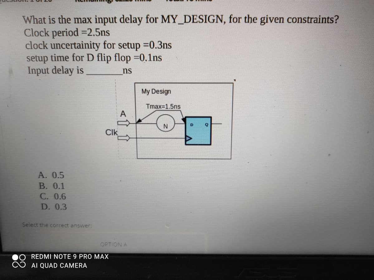
What is the max input delay for MY_DESIGN, for the given constraints? Clock period =2.5ns clock uncertainity for setup =0.3ns setup time for D flip flop =0.1ns Input delay is ns


Q: 25-2: For the following master-slave structure of two edge-triggered flip-flops, D and T, complete…
A: The diagram of Flip-Flop is: Both flip-flops have the same clock pulse. The signal A is input to D…
Q: Which of the following is/are true of a synchronous counter? The sameclock signal is sent to all…
A: I. True, In synchronous counters all the flip flops are connected to the same clock signal. There is…
Q: Explain the operation of serial input and serial output using four-bit shift register with D…
A: Shift registers are used to stored the data. In serial In and Serial out shift register, data is…
Q: Determine the Q and Q' output waveforms of the D flip-flop with D and CLK inputs are given in figure…
A: Digital circuits can either be combinational circuits or sequential circuits. Sequential circuits…
Q: Write down the truth table, characteristic table and excitation table of a SR flip flop, where the…
A: we need to determine truth table, characteristic table and excitation table for SR flip flop.
Q: 1. Design a 3-bit ripple counter using JK flip-flop. State Table: 3-bit ripple counter Present State…
A: Ripple counter: It is type of the asynchronous counter. The circuit is ripples when the clock pulse…
Q: 2- Design synchronous counter using positive edge J-K flip flop to count the following states…
A:
Q: 1. What is D-Ilatch? What is its purpose? Draw its combinational gates and write its truth table? 2.…
A: Delay flipflop circuit and truth table
Q: D- D1 Q1 Data Path D2 Q2 FF1 FF2 CLKA CLKB Routing Delay SYSCK For a given sequential circuit as…
A: Flip flop is a latch with additional control input (clock or enable ). A flip flop is used to store…
Q: Discussion: what is the effect the activating the (preset and clear) on the output state for J-K…
A: Preset and Clear are the two asynchronous inputs are provided to all flip-flops to make the output…
Q: a- Plot the SR Latch circuit b- Explain the behavior of SR latch C- How to convert SR latch into D…
A: Bartleby has policy to solve only first question and its first 3 subparts only.
Q: Problem_#04] Construct a timing diagram showing sixteen clock pulses. HIGH Jo J2 Q2 CLK C C C Ko K1…
A: Part (6): In the synchronous counter, all the clock inputs of the flip-flops are connected with the…
Q: An asynchronous state machine has two inputs (X1 نقطتان )2( and X2) and one output (Z). The output…
A: The solution is given below
Q: What is the main operation of thes logic arcuit? A F B O XOR O Flip-Flop O Universal ANDing O Latch
A:
Q: a) What type of counter does the circuit implements? b) Describe its output sequence? c)…
A:
Q: 1. Convert SR flip-flop to JK flip-flop. 2. The following serial data have been applied to the…
A: The flipflop of one type can be realised by using another type. The output of flipflop can be…
Q: What is the type of the flip flop? Present state Next state output output At delay cross coupled D…
A: Based on the digital circuit
Q: 2. An asynchronous down counter was build from four JK flip flop with clock of first flip flop is…
A: "Since you have asked multiple questions, we will solve the first question for you. If you want any…
Q: Verify the truth table of master salve flip flop using logic gates
A: Verify the truth table of master salve flip flop using logic gates
Q: Answer the following questions given the timing diagram of a certain flip-flop which has a clock of…
A: In this question, choose the correct option What is the time take to output after triggering.
Q: Q4/ (Answer One Only) from the following : 1- Design synchronous counter using negative edge D- type…
A:
Q: What is the vhdl code for 4-bit universal shift register using d flip flop with the following…
A: VHDL code for 4 bit library ieee;use ieee.std_logic_1164.all;entity pipo isport (clk:in…
Q: Design a 4-bit synchronous counter that counts in 2,4,2,1 code. The counter shall count all Odd…
A: SEQUENTIAL LOGIC CIRCUITS: Sequential Logic circuits, unlike Combinational Logic circuits, have some…
Q: ow do you draw flip flops and latch being drawn in boolean algebra? What happens if change them to…
A: Flip-flop- It is one bit storing element. The output of combinational circuit depends only on…
Q: Answer the following questions given the timing diagram of a certain flip-flop which has a clock of…
A: In this question, Choose the correct option What is the type of triggering /clocking used? as…
Q: 3 Consider a T flip-flop constructed from the negative edge triggered JK flip-flop with active low…
A: The solution is given below
Q: An asynchronous state machine has two inputs (X1 and X2) and one output (Z). e output is the same of…
A:
Q: 7−bit shift register using JK flip-flops
A: Shift Register It is a type of sequential logic circuit that can be used for the storage and…
Q: Explain the distinction between synchronous and asynchronous inputs to a flip-flop.
A: Synchronous input In synchronous inputs, the signals which are input to the flip-flops are highly…
Q: Design a Asynchronous Up counter that start it’s counting from zero and ends at 13 and again starts…
A: The counter should count up to 13, It is a MOD-13 Counter log2(13) = 3.7 Hence it required 4 flip…
Q: Design a binary counter that counts from 0 to 5. At each clock pulse, 3 lights will be ON and 3…
A: Given data: A binary counter that count from o to 5. 3 light will be ON and 3 light will be OFF.…
Q: Discussion: what is the effect the activating the (preset and clear) on the output state for J-K…
A: a) Effect of activating the (present and clear) on the output state for J-K flip flop The…
Q: erify the truth tables of JK Master-slaves flip flop with its logic gates?
A: consider the given question;
Q: The first flip-flop of a ripple counter is clocked by none of the mentioned logic 1 O the Q' of the…
A:
Q: Construct a synchronous 3-bit Up/Down counter with irregular sequence by using J-K flip-flops. The…
A:
Q: DESIGN 1-6 SYNCHRONOUS UP COUNTER USING JK FLIP-FLOP 7476 IC REQUIRED: A) EXCITATION TABLE OF JK F-F…
A: The solution is given below
Q: Illustrate a complete timing diagram (i.e., one entire cycle back to the starting states) for a 4…
A: 4-bit ripple counter using T flip-flops with negative edge clock triggers:
Q: Q4(a) Determine the Q output waveform of the flip flop in the Figure Q4(a). Assuming that the…
A:
Q: A binary counter that will count 0 to 5 is wanted to be designed. A floating light line including 6…
A: JK flip flop diagram given below shows the basic structure which consists of the clock, clear and…
Q: An asynchronous state machine has two inputs (X1 and X2) and one output (Z). he output is the same…
A:
Q: a- Plot the SR Latch circuit b- Explain the behavior of SR latch С- How to convert SR latch into D…
A: Bartleby has policy to solve only first question and first 3 subparts of a question. For rest…
Q: a) Draw a circuit diagram for the synchronous parallel transfer of data from one three-bit register…
A: (a)Circuit for synchronous transfer data from one 3 bit register to another J-K flip flop.
Q: How to use Flip Flops to design a six bits Parallel in /parallel out shift register ? Explain with…
A: FIND: Six bits parallel in / parallel out shift register by using flip flop.
Q: How 8 bits register can be formed with D type flip-flops
A:
Q: write simple assignment statements vhdl code for 4 bit universal register using D Flip Flop with…
A: // D flipflop//library IEEE;use IEEE.STD_LOGIC_1164.ALL; entity d_flip_flop is Port ( D : in…
Q: 1) The following waveform are applied to the J-K flip flop with negative edge clock pulse. Assuming…
A: We need to draw output waveform for jk flip flop .
Q: 19. In a negati ve edge triggered T-flip flop, before the negative edge, input is 0 and output is 1.…
A: As per the guidelines of Bartley we supposed to answer first three subpart only.
Q: 1) Draw a 4-bit parallel-in parallel-out register using JK Flip Flops 2) Draw a 4-bit shift right…
A:
Q: Suppose the machine is initialized to its starting state '00' and then processes the input values:…
A: The given truth table is Use the truth table and the input sequences to find the next states and…

Step by step
Solved in 2 steps


- Suppose some hypothetical system’s control unit has a ring (cycle) counter consisting of some number of D flip-flops. This system runs at 1GHz and has a maximum of 10 microoperations/instruction. Q.How long does it take to execute an instruction that requires only four microoperations?Illustrate a complete timing diagram (i.e., one entire cycle back to the starting states) for a 4 bit ripple counter created using T flip-flops with negative edge clock triggers.Implement the following Boolean function by using 4x1 multiplexer. ����(?, ?, ?, ?) = Ʃ?(1,3,5,6,8,11,14) Construct a logical circuit of 64 × 1 multiplexer using 4 × 1 multiplexer. Construct a priority encoder circuit of 8x3. Design a 4-bit BCD to Gray Code Converter by using Programmable Array logic.
- Design a three bit synchronous binary counter that counts two by two with T-flipflops,continously. Output should be one when the counter equals maximum number.a. Draw the exitation table b. Draw the corresponding state diagram. c. Tabulate the state table for the sequential circuit. d. Draw the logic diagram of the circuit.S Display will be designed for a thermometer. The display will show that degree for minimum temperature and 99 degrees for maximum temperature. According to this; a) What is the number of bits that will be needed in the binary code to express the temperature? b) What are the binary, octal and hexadecimal equivalents of 95 degrees? () What is the BCD representation of 95 degrees? d) What is the hex equivalent of this temperature when it shows 111 degrees octal? e) If the thermometer showed a temperature between -99 and +99 degrees, how many bits would we need?You are asked to design a synchronous counter that will count the sequence 1 > 2>3>1. (a) Represent these decimal numbers in 2 bits binary numbers. (b) Write down the state table. (c) Find the functions for the next state of the state table using K-map. (d) Draw the circuit (You need to consider D flip-flops as memory unit).
- Analyze the timing diagram. Which flip-flop is being used? CLK PRE CLR J,K Q 1 0 1 0 1 0 a b e It is negative clock pulseFor the path in the following figure, determine which latches borrow time and if any setup time violations occur. Do this for a cycle time of 1000 ps and a duty cycle of 50%. Assume for the latches and flip-flops the setup and delay time is 100 ps. Use Δ1 = 250 ps , Δ2 = 600 ps, Δ3 = 600 ps. Will the circuit function correctly with the given combinational circuit delays? Explain.Question 5(a) ) (i)What is a flip-flop? What is the difference between a latch and a flip-flop? List out the applications of flip-flop (ii) In a JK Flip-Flop, what is the meaning of toggle, and how does it happen (b) Kindly design a Master-slave J-K flip-flop using NAND gates only and state race-around condition, and how it can be eliminated in a Master-slave J-K flip-flop? (c) In your own understanding kindly demonstrate why in digital logic family, ECL has the lowest propagation delay time?
- Draw the Moore and Mealy State Diagram of a Finite State Machine thatfunctions as a Binary Sequence Detector for the following sequence:a. 01011b. 101 and/or 010Obtain the State Table for each of your diagrams?Design a binary counter that counts from 0 to 5. At each clock pulse, 3 lights will be ON and 3 lights will be OFF. Use JK flip flops.Steps for solution:-> State diagram-> State table-> K-map reductions-> designIn a home security system, the main door (O) of home is controlled by a logic operation with the help of RFID card. the Owner, Mrs. Owner, Security Guard and Guest have a designated RFID card - Owner with card W, Mrs. Owner with card X, security guard with card Y and guest with card Z. Whenever, any of the card is NOT inserted, Door remains Closed; when, all the cards are inserted together, the Door is opened. Consider, card NOT inserted as Logic Low (0), card inserted as High Logic (1), door open as Low Logic (0) and door close means High Logic (1).(i) Identify the logic based on the problem statement(ii) Develop the truth table (W, X, Y & Z – inputs, O – output)(iii) Find the Standard SOP and Standard POS expression(iv) Find the Simplified SOP expression using KMAP.(v) Design the system using basic logic gate.