A3. Connect the circuit as shown in Fig. 1.3. With SW1 and SW2 apply the states shown in Table 3. Record the output state for each set of input states by observing the LED indicator. Table 3 swi SWi OUTPUT 1 SW2 0- Fig. 1.3 1 1
Q: 00 A-00 11 с-10 01 10 Z-0 Z-0 Too 01 10 01 10 11 01 00 10 В-01 D=11 Z-1 00 Z-1 1. Draw the state…
A: The solution for the above given question is given below:
Q: Design an appropriate combinational circuit that implements a digital system with the following…
A: Design a combinational circuit which take 4bit input and it has 7 outputs to which connect with the…
Q: Given the expression below, build the equivalent digital circuit NAND implementation. X = AB+ CB +…
A:
Q: Draw the circuit and obtain the truth table of the VHDL module below module SAM(a, b, c, M, S);…
A: We need to draw the circuit and obtain the truth table of the given VHDL module.
Q: Compute the output frequency, fout for the sequential circuit given in Fig. Q2(b)(i). Assume a 48…
A: Below I have provided the handwritten solution to the given question
Q: 3. Implement a BCD to seven segment decoder for a common anode seven segment display. (It means that…
A: In a common anode display, every one of the LED segments' anode connections are connected to logic…
Q: 2) For the counter shown in Fig. 15(a), sketch the output waveforms (A, B and C) for the inputs…
A: Timing Diagrams : From the given logic circuit we can draw timing diagram as follows.
Q: SECTION D: DIGITAL LOGIC 1. Draw the logic circuit represented by the following expression: a)…
A: Logic Circuit is the pictorial representation of the Boolean expressions. Each logical operation is…
Q: Question 5 What type of state machine is this circuit and why? 2) Write equations for flip-flop…
A: A state machine reads a set of inputs and changes to a different state based on those inputs.
Q: Task 1: Circuit analysis Find the Boolean expression that represents the outputs x and y shown in…
A: LOGIC GATES
Q: Analyse the following circuit BEBERU Qo J Q Q, J Q Q2 J Q DC C Q, K Q Q2 K Q0- K. K Q CLK a)…
A: Given Sequential circuit contains, 3 J-K flipflops Three states are Q0, Q1, Q2 Assume that, the next…
Q: 4) of which only 10 are used. Analyze the circuit and determine the next state for each of the other…
A: The BCD ripple counter shown the following Figure has four flip-flops and 16 states, of which only…
Q: a. What is the Boolean expressions for the circuits A and B? b. What is the Truth Table for the…
A:
Q: Simply the boolean expression and draw the equivalent circuit
A:
Q: For the following State table: 1. Draw its equivalent state diagram 2. Write a VHDL code that…
A: ANSWER:-
Q: Problem You are given the following Digital circuit. out4 CLK CLK CLK X X out2 CLK (Ctrl) out2 DO x…
A: Q2)
Q: 1. Draw the state diagram and state table for the following circuit: D. D. Clock X- Present state…
A: Solution: we make truth table: ============================================
Q: Consider the below sequential circuit to determine the values of L M, N, Q in the corresponding…
A: Lets see the solution.
Q: Q2: A- Here's a table showing the ten and tro for each of the components in the circuit bellow.…
A:
Q: Y- A a. What is the transition table of the sequential circuit? b. What is its excitation and output…
A: Solution:
Q: What is the difference between a combinational circuit and sequential circuit? Give example of each.
A: Computer circuits consist of combinational logic circuits and sequential logic circuits.
Q: I. Write down the state equations. II. Write down the output equations. III. Write down the state…
A: 1. Here first we need to find input equation to all the flip-flop from the diagram DA => B.C DB…
Q: 2: Draw the output waveforms (S, X, and Y) for the below sequential circuit b assuming the…
A:
Q: Please see attachment.
A: In the given expression, three inputs are given – A, B, and C.A bar above the inputs is…
Q: a) Draw the state table of the synchronous sequential circuit, b) Derive the next state equations…
A: Answer in Step 2.
Q: 1. In the shown digital circuit F is equal to: а. 0 b. 1 c. x +y d. None of the above y. So 4 x I…
A: Here, we are going to compute the value of circuit F. Select lines are x and y.
Q: [Q4] For the following circuit, (a) determine the state table; (b) Sketch the state graph; (c)…
A: According to the information given:- We have to sketch the ASM flowchart of the given circuit.
Q: 1. Examine the circuit in Figure 2.1 and write the Boolean expression for the output F. F ABC
A: We are given a logic circuit for which we are going to find out the boolean expression. First I will…
Q: 13. Which of the following determines the output of a combinational circuit? A. its input values…
A: COMBINATIONAL CIRCUITS: Combinational circuits are those circuits which are formed using the basic…
Q: What type of device is shown in Fig. B1 if the waveforms illustrated are present at its CK and Q…
A: Answer : 1. it is BI-STABLE
Q: 2) For the counter shown in Fig. 15(a), sketch the output waveforms (A, B and C) for the inputs…
A:
Q: 2. Complete each circuit below by adding the needed devices so the output is high or low for all…
A: The solution for the given question is given below:
Q: A FSM has two flip flops with outputs A and B and inputs D(A) and D(B) respectively (as in the…
A:
Q: 1. Design the state diagram and create the state table for a synchronous to detect the sequence…
A: GIVEN:
Q: 3. For the multiplexer shown in the figure, write the truth table and draw the output waveform. 4x1…
A: In this question, we have to draw the output waveform and also write the truth table. In given 4x1…
Q: 1. In the shown digital circuit F is equal to: а. 0 b. 1 c. x +y d. None of the above y So 4 x I MUX…
A:
Q: 5. Determine Vo and In for the circuit in figure below; +10 Vo Page 3 of 5 6. Determine Vo for the…
A:
Q: Draw the circuit diagram to output F given in the expression above by referring to schematics for…
A:
Q: 1. In the shown digital circuit F is equal to: а. 0 b. 1 c. x +y y- So d. None of the above 4 x I…
A: We need to find the output function.
Q: Exercise 2: Determine the output F1 (X, Y, Z) and F2 (X, Y, Z) of the below circuit: 1 4 x 1 MUX 1-…
A: In this question, we are given 2 mux whose output is connected to a half adder. Logic: we will first…
Q: 1. For the circuit below, sketch the output waveform Q with the given input and clock signals.…
A: 1.output wave form Q with the given input 2.SR flip-flop to flip-flop
Q: 9 Draw a frequency divider "divide by 2 and "divide by 4" logic circuits as a single circuit…
A:
Q: draw a QPSK demodulator circuit using different circuit component
A: QPSK demodulator circuit:
Q: Consider the below sequential circuit to determine the values of state diagram of the circuit. Note:…
A: Lets see the solution.
Q: 1. Find and draw the state table E. Find and draw the excitation table . Find and write the FF's…
A: Please give positive ratings for my efforts. Thanks. As per guidelines, we are allowed to answer…
Q: Q8/ Draw the state diagram and state table of a circuit that serially check non BCD code. The output…
A:
Q: Problem 1. Draw the waveforms of Q0, Q1, Q2 (all initialized to zero) What is the countering…
A:
Q: Q2. Design a sequential circuit with two JK flip-flops A and B and two inputs E and x. If E=0, the…
A: Sequential circuit with two JK flip-flops A and B and two inputs E and x. If E=0, the circuit…
Q: For the following inputs, the selector digits of the given multiplexer circuit should be (s1,s0)=( )…
A: We are given 4x1 multiplexer and values of 4 inputs ( I0 to I3). As we know that output Y select an…
Study Table 3. What logic is being performed?
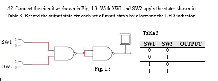
Trending now
This is a popular solution!
Step by step
Solved in 2 steps
- F =A'BC'+A'CD'+ACD+AB'C'D' Draw the Logic Gates diagram please Need AsapDesign the simplest circuit that has three inputs, a, b, and c, which returns an output value of 1 whenever g and b are complements of each other or b and c are complements of each other, otherwise the output is 0. Realize the circuit using 4input , 3output PALDraw the circuit and obtain the truth table of the VHDL module below module SAM(a, b, c, M, S);input a,b,c;output M;output S;wire d,e,f;xor(S,a,b,c);and(d,~a,b);and(e,b,c);and(f,~a,c);or(M,d,e,f);endmodule
- Please show solution to answer The state diagram for a sequential circuit appears in the following figure. Make a state assignment for the circuit using 3-bit codes for the six states; make one of the code bits equal to the output to save logic, and find the encoded state table. The next states and outputs are don’t cares for the two unused state codes.Draw the circuit diagram to output F given in the expression above by referring to schematics for 2-2) and 2-3). Use the space below to draw both the IC with pin assignments and a circuit schematic. Using a single 7400 IC construct a circuit to output the following Boolean function: F = AB + CDIdentify the state diagram operation and find its output sequence for the following input sequence X=0101-1100-101-0000 the circuit accepts input bits from LSB to MSB
- 4. Draw a JK Flip Flop circuit configured to automatically toggle between the outputs every 0.5 seconds. On what settings and inputs did you draw to cause this to happen? 5. Draw a graph to express function of the output Q in the previous question. Let the independent variable be time elapsed (seconds) and the dependent variable be voltage level (V). What does this graph resemble?Computer Science Lab 8 PWM in C Generate PWM codes in C using the ACLK to create a wave form of 150Hz with duty cycle of 20% and 75%. Run in low power mode 3. Connect each wave to the red LED and observe the brightness difference. Display each wave with an oscilloscope and include the display in the report.Draw a state diagram for an FSM without inputs. Three outputs include a, b, and c. abc must exhibit the following sequence: 000, 001, 010, 100, repeat. The output only changes on a rising clock edge. The initial state must be 000.
- Draw a state diagram for an FSM without inputs. Three outputs include x, y, and z. xyz must exhibit the following sequence: 000, 001, 010, 100, repeat. The output only changes on a rising clock edge. The initial state must be 000.6. For the showa device, determine the output for the inputs 0110 , \[ \$ 1=1, S 0=1 \text {, and Enable }=0 . \] A. 1 . B. 0. C. Hj-Z. D. Don't Care. 7. Implement the Half-Adder circuit (S and C) with a decoder (use a block diagram for the Decoder) and the minimum number of gates. 8. Design a combinational circuit with three inputs and the output is 1 when the binary value of the inputs is greater than 4 . The output is 0 otherwise In yowr design, you have to do the three steps of the design procedures as follows: - Derive the truth table - Reduce the circuit using K-map - Draw the resultant logic circuit. 9. Use the dawa 8-to-1 multiplexer w implewest the functionfrepersented by the following truth wable. Please give proper explanation and typed answer only.Design a combinational circuit with three inputs x, y, z, and three outputs a, b, and c. When the binary input is 0, 1,2, or 3 , the binary output is 1 greater than the input. When the binary input is 4, 5, 6, or 7, the binary output is one less than the input.