(d) A TTL gate has a following actual voltage level values: VH (min) = 2.25V and Vn (max) = 0.65V Assuming it is being driven by a gate with Von (min) = 2.4V and Vor (max) = 0.4V, determine the HIGH and LOW level noise margins.
(d) A TTL gate has a following actual voltage level values: VH (min) = 2.25V and Vn (max) = 0.65V Assuming it is being driven by a gate with Von (min) = 2.4V and Vor (max) = 0.4V, determine the HIGH and LOW level noise margins.

Chapter22: Sequence Control
Section: Chapter Questions
Problem 6SQ: Draw a symbol for a solid-state logic element AND.

Related questions
Question
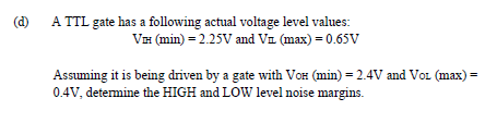
Transcribed Image Text:(d)
A TTL gate has a following actual voltage level values:
VH (min) = 2.25V and Va (max) = 0.65V
Assuming it is being driven by a gate with VoH (min) = 2.4V and Voz (max) =
0.4V, detemine the HIGH and LOW level noise margins.
Expert Solution
This question has been solved!
Explore an expertly crafted, step-by-step solution for a thorough understanding of key concepts.

Step by step
Solved in 2 steps

Knowledge Booster


Learn more about
Need a deep-dive on the concept behind this application? Look no further. Learn more about this topic, electrical-engineering and related others by exploring similar questions and additional content below.Recommended textbooks for you