Example 2 : Find the current flowing through R1, R2, R3, R4 and Vx if Vs = 10 V, R1 = 1kQ, R2 -330Ω, R-2.2kΩ and R-670Ω R1 R3 a) Assuming Ideal diode b) Silicon Diode c) Germanium diode d) Reversing the Power supply Vs and all R4 diodes are silicon R2
Example 2 : Find the current flowing through R1, R2, R3, R4 and Vx if Vs = 10 V, R1 = 1kQ, R2 -330Ω, R-2.2kΩ and R-670Ω R1 R3 a) Assuming Ideal diode b) Silicon Diode c) Germanium diode d) Reversing the Power supply Vs and all R4 diodes are silicon R2

Delmar's Standard Textbook Of Electricity
7th Edition
ISBN:9781337900348
Author:Stephen L. Herman
Publisher:Stephen L. Herman
Chapter29: Dc Generators
Section: Chapter Questions
Problem 1PA: You are working as an electrician in a large steel manufacturing plant, and you are in the process...

Related questions

Question
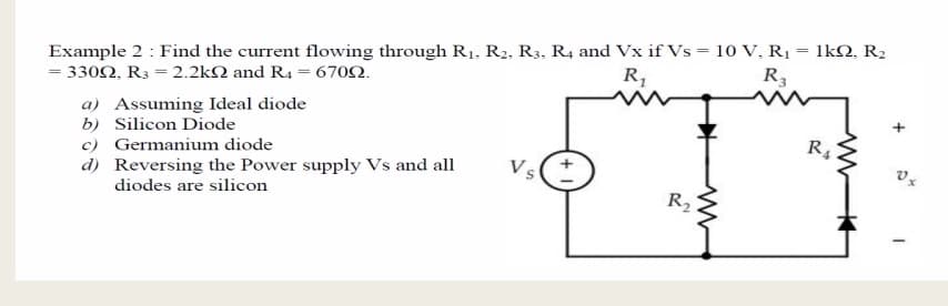
Transcribed Image Text:Example 2 : Find the current flowing through R1, R2, R3, R4 and Vx if Vs = 10 V, R1 = 1kQ, R2
= 3302, R3 = 2.2k2 and R4 = 6702.
R,
R3
a) Assuming Ideal diode
b) Silicon Diode
c) Germanium diode
d) Reversing the Power supply Vs and all
diodes are silicon
+
R
Vs
R2
Expert Solution
This question has been solved!
Explore an expertly crafted, step-by-step solution for a thorough understanding of key concepts.

This is a popular solution!

Trending now
This is a popular solution!

Step by step
Solved in 3 steps

Knowledge Booster


Learn more about
Need a deep-dive on the concept behind this application? Look no further. Learn more about this topic, electrical-engineering and related others by exploring similar questions and additional content below.Recommended textbooks for you
Delmar's Standard Textbook Of Electricity
Electrical Engineering
ISBN:
9781337900348
Author:
Stephen L. Herman
Publisher:
Cengage Learning
Delmar's Standard Textbook Of Electricity
Electrical Engineering
ISBN:
9781337900348
Author:
Stephen L. Herman
Publisher:
Cengage Learning