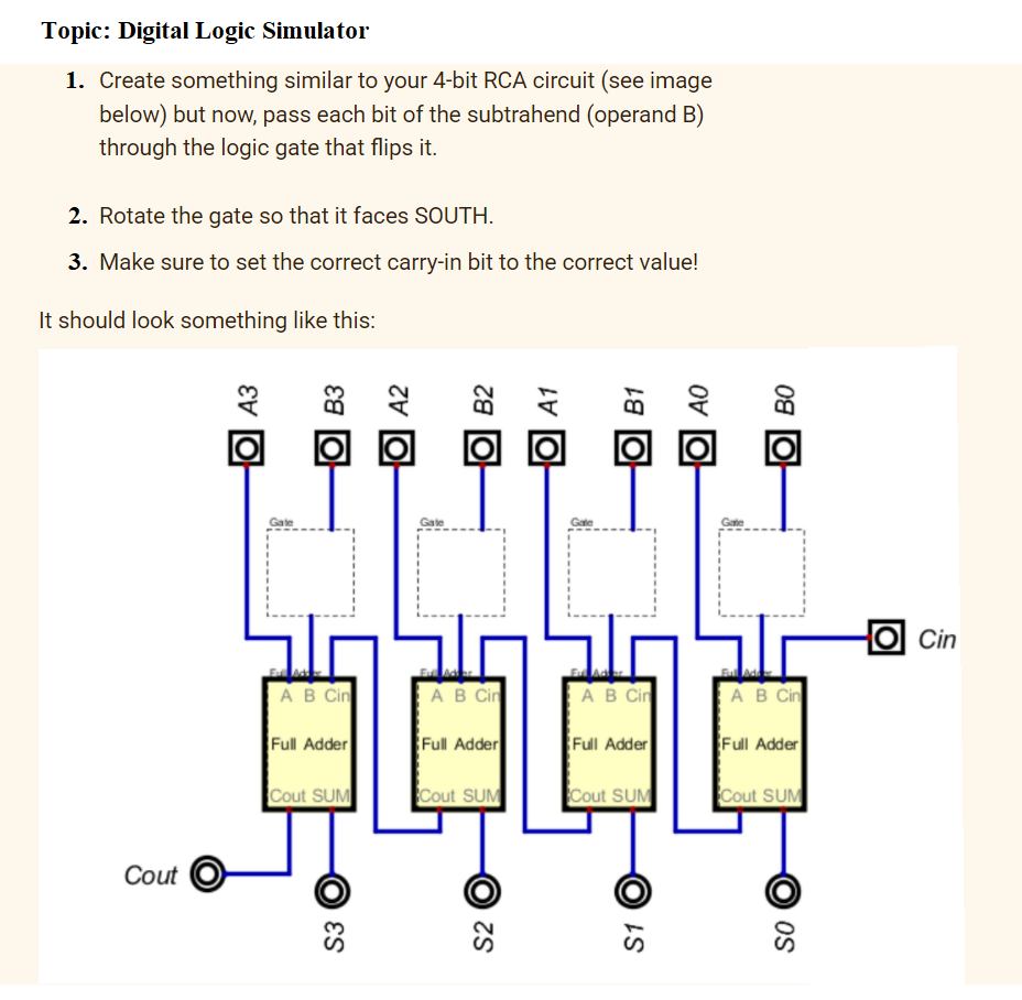
Fill-in the blank boxes with the correct LOGIC GATE/ Full/Half Adder


Q: 1) Implement a full adder with two 4 x 1 multiplexers. 2) Draw the logic diagram of a 2-to-4-line…
A: The solution of the following questions are
Q: 3.(a) Make a truth table for this given logic gate, as shown in the figure. Show the steps. What is…
A: “Since you have asked multiple questions, we will solve the first question for you. If you want any…
Q: A B 2
A: The given data is as follows:-
Q: Distinguish between Half Adder and Full Adder as applied in combinational logic circuit
A: In digital electronics circuit are classified in two categories: Combinational circuit Sequential…
Q: 1. A standard TTL gate performs what logic function for positive logic? 2. If all inputs of a TTL…
A: ANSWER (1) A standard TTL gate perform NAND LOGIC function for Positive…
Q: 2) The output of a logic gate is 0 when all its inputs are logic 1. The logic is either (A) a NAND…
A:
Q: Implement Four-to-one-line multiplexer with Logic diagram and Function table.
A:
Q: QII Determine the modulus of the logic circuit (counter) shown in figure below and write its…
A:
Q: 2- Construct a full-Adder logic circuit by using NAND gates only. 3- Construct a full- Subtractor…
A: The solution of the following questions are
Q: Distinguish between Half Adder and Full Adder
A: Adder: Adder is digital circuit that performs addition operation of numbers. In computers adders…
Q: Implement 1-to-8line demultiplexer with active low enable input using logic gates
A: Demultiplexer:- It is a combinational circuit that is the inverse of the multiplexer. It performs…
Q: 1. A standard TTL gate performs what logic function for positive logic? 2. If all inputs of a TTL…
A: TTL GATE: TTL(Transistor- Transistor logic), is mainly built up from a Bipolar junction transistor…
Q: Which logic family is fastest and which ha low power dissipation?
A: #ECL (Emitter-Coupled Logic) is the fastest among all logic families. Reason: The emitters of many…
Q: Q.4 Draw the logic diagram to implement the following expression with minimum number of NAND gates.…
A: The solution is provided in the following section:
Q: Discuss the pin diagram of any logic gate? Explain how the NAND gate can be used to derive the other…
A:
Q: 'a- Con for the following Circuit and identify that canse replace the circu a single logic gate A.
A:
Q: Implement using full adder 3 × 8 complementary output decoder (decoder -74138 IC) and appropriate…
A: Explanation: The truth table for Full adder is A B C Sum Carry Decimal place 0 0 0 0 0 0 0 0…
Q: For the state diagram given below, create the state table and design the sequential circuit with SR…
A:
Q: Consider a family of logic gates that operate under the static disci
A: given values VI=1.5V ,VOL=0.5V, VIH =3.5V, and VOH=4.4V then the ouput voltage as
Q: 4. For the NOR gate function shown below A Da B. Do a) Write the switching expression for the…
A:
Q: A B What logic gate has the same function as the circuit above? O XOR O XNOR O AND O NAND O OR O NOR
A: Find out the out put of each logic gate And Simplified it for getting equilent logic function . out…
Q: Design and draw the logic diagram for a two-input NAND gate using one two-input AND and one NOT…
A:
Q: 4.) Using 4 Full Adders, one 2x1 Multiplexer, 3 D-latches, and any number Digital Logic Gates (any…
A: F = AB¯ + A¯B F = CD¯ + C¯D¯ F = Sum A , B F = Sum A , B , C , D This is done by using 4×1 Mux and 2…
Q: Draw the logic diagram of a 2-to-4-line decoder using (a) NOR gates only and (b) NAND gates only.…
A: The two to four decoder can be designed by using the universal gate and this can be achieved by…
Q: A certain logic gate has a VOL(max) = 0.45 V, and it is driving a gate with a VIL(max) = 0.75 V. Are…
A: This question is from "Digital Electronics". Under which we are going to study the basic working…
Q: Q1// What are the difference between Logic Devices and Programmable Logic Devices? Q2// Explain the…
A: As per the honor code I will answer only first three. Kindly repost the other questions again. THANK…
Q: What is the one-bit half adder's purpose? What is the total number of inputs and outputs? What logic…
A:
Q: How to implement flip flop using nor logic gates and also with nand logic gates? Also explain…
A: A flip flop also known as bi-stable multivibrator having two stable states. It can remain in either…
Q: subject: Digital Logic &Design Q: Describe the operation of a basic parity generating and checking…
A: A message signal is transferred from the sender to the receiver end. The signal is transmitted…
Q: Explain the working of 7-Segment Display. What it can display and how logic reduction is carried out…
A: According to the question, we need to explain the working of the 7-Segment Display. What it can…
Q: Q.6 Describe the operation of a basic parity generating and checking logic.
A: In digital systems, the parity generator is a combinational logic circuit. this logic circuit is…
Q: Draw in Table 3 the circuit schematic of each segment using the basic logic gates in kmap
A: According to the given question, The logic diagram of the above-given SOP equation can be drawn by…
Q: Consider a family of logic gates that operate under the static discipline with the following voltage…
A:
Q: Design 3 systems that represent minterm 30 for a 5-input system: 1.-using logic gates, with a…
A: According to the question, we need to design 3 systems that represent minterm 30 for a 5-input…
Q: Design the circuit of OR gate with three input using simple logic module ?
A: Given that: The number of inputs =3 Output =1
Q: Logic gate No. 5 * A B F
A: Please find the detailed solution in below images
Q: Define a 2-bit demultiplexer to be a circuit whose single input line is steered to one of the four…
A:
Q: is there a way for the output voltage of a comparator to be the same as its supply voltage? im…
A:
Q: : Describe any two Digital Logic Gate with its truth table and high light it properties
A:
Q: Consider a family of logic gates that operate under the static discipline with the following voltage…
A: We need to find out voltage for different conditions .
Q: f the output field devices. B)The choice of normally-open and normally-closed instructions for
A: Given: The answer is shown as:
Q: List only TWO features of Transistor Transistor Logic (TTL) series and draw the circuit diagram of…
A: There are various categories of digital circuit, depending on different technologies. The categories…
Q: 5.3 A clock signal as a continuous sequence of pulses is applied to a logic gate and is to be…
A: Given a clock signal (clk) of continuous pulses is applied to logic gate i.e I am taking this clock…
Q: Y%=D イ DO
A: By simplifying the circuit y= ABC which is 3 input AND gates.
Use any digital logic simulator
Fill-in the blank boxes with the correct LOGIC GATE/ Full/Half Adder

Step by step
Solved in 2 steps with 2 images


- Sketch 3-input XOR/XNOR functions using DCVS (differential cascade voltage switch) and CPL (complimentary pass transistor logic), compare their speed, power, area, and explain your answers1:The output of a logic gate is 1 when all the input are at logic 1 and a . OR and EX - NOR Gate b . AND Gate and EX - OR Gate C. OR and EX - OR Gate d . NAND and OR Gate 2: Choose an application of A / D convertor a. Sonar systems b. Radars and Jammers C. Digital Audio apllications d. Encoders 3: Find the simplification of AB + B ( B + C ) + C ( B + C ) a. C + A b. B + C c. 1 d. A + 4: Choose a correct number of input lines for a decoder which has 128 output lines a . 14 b . 7 c . 1 d . 128 6: Select a suitable example for sequential logic circuit . a . Encoder b . None of the given choices c . Counters d . PALWhat is a transmission gate? Draw its circuit circuit diagram. How does it operate? What is the need for a transmission gate? What is it disadvantage?
- choose the correct answer If a two-input logic gate produces a output of logic HIGH, only if both inputs are different, then the logic gate is? a. IC 7400 b. IC 7486 c. IC 7408 d. IC 7432Use Digital Logic Simulator Fill-in the blank boxes with the correct LOGIC GATE/ Full/Half Adder1- What does the VOH parameter of a logic IC refer to? a) The highest permissible output voltage. b) The lowest output voltage recognized as logic 1. c) The highest output voltage recognized as logic 1. d) The highest output voltage recognized as logic 0. 2- Which of the following refers to the noise margin of a logic gate? a) The difference between VIH and VOL b) The difference between VOH and VOL c) The difference between VOH and VIH d) The difference between VIH and VIL 3- How many 74LS00 NAND gate inputs can be driven by a 74LS00 NAND gate outputs Refer to data sheet of 74LS00, the maximum values of IOH = 0.4 mA, IOL = 8 mA, IH = 20 μA, and IL = 0.4 mA. 4- The data sheet of a quad two-input NAND gate specifies the following parameters: IOH (max.) 0.4 mA, VOH (min.) 2.7 V, VIH (min.) =2V, VIL (max.) 0.8 V, VOL (max.) 0.4 V, IOL (max.) 8 mA, IL (max.)=0.4 mA, IIH (max.)-20µA, ICCH (max.) 1.6 mA, ICCL (max.) 4.4 mA, tpLH =pHL=15 ns and a supply voltage range of 5…
- Discreet Mathematics Create the logic circuit diagram for F= XY’ + XZQ1. Read the following description concerning a logic circuit, and then answer Subquestions 1 and 2. Figure 1 shows a logic circuit that is used as a control system for an electronic device. The logic circuit has three inputs (X, Y and Z) and one output (F). As shown in Figure 1, the logic circuit has a feed back line, by which the last output F is fed back and is used as the current input to the NAND gate. Therefore, the current output F is determined by three current inputs X, Y and Z and the last output F. In this control system, among three inputs X, Y and Z, at most only one input can change its value on each clock cycle. (Feed back line) Figure 1 The logic circuit Meanings of the logic gate symbols used in Figure 1 are as follows: AND gate NAND gate OR gate NOR gate Figure 2 shows sample input/output status of the logic…logic circuitjust draw the graph
- Develop an assembly code for an LED 8-bit binary counter, where LEDs are connected to the Port 2. Here are the instructions, (1) counter should start when a HIGH input is present at P1.0 and stop the counter when a LOW input is present/read at the P1.2. (2) Draw the circuits diagram. Hint: Switch connected to P1.0 should pass HIGH when switch is pressed, where as switch connected to P1.2 should pass LOW when switch is pressed. Accordingly adjust your circuit connections and the code.There are 5 gates in a metrobus, 1 of which is to get on and 4 to get off. The number of passengers inside is desired to be seen on the LCD connected to the P2 port. Get-on gate is controlled by the P0.2 while get-off gates are controlled by the P0.3, P0.4, P0.5, and P0.6. The sensors generate Logic-1 while passing passengers. Since the passenger carrying capacity of the metrobus is 294, if the number of passengers exceeds the number of 294, the warning LED connected to the P0.7 pin is required to light up. Since other pins of P0 are used for other purposes, it is not desired to be changed. Can you write the answer with assembly code using 8051 - AT89S8253 architecture?1. Design 8086’s memory system consisting of 64K bytes of ROM using32KX8 chip. The memory is to reside over the address range 60000Hthrough 6FFFFH. Select suitable address maps.2. If the memory chip size is 1024 X 4 bits, how many chips are required tomakeup 2K bytes of memory?3. Interface 16 K word of memory to the 8086-microprocessor system.Available memory chips are 8 K X 8 RAM. Draw the memory table.