For a master-slave J - K Flip - Flop with the inputs below, sketch the Q output waveform. Assume Q is initially low. Assume the Flip - Flop accepts data at the positive-going edge of the clock pulse.
For a master-slave J - K Flip - Flop with the inputs below, sketch the Q output waveform. Assume Q is initially low. Assume the Flip - Flop accepts data at the positive-going edge of the clock pulse.

Chapter22: Sequence Control
Section: Chapter Questions
Problem 6SQ: Draw a symbol for a solid-state logic element AND.

Related questions
Question
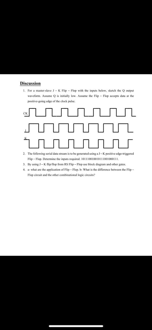
Transcribed Image Text:Discussion
1. For a master-slave J- K Flip - Flop with the inputs below, sketch the Q output
waveform. Assume Q is initially low. Assume the Flip - Flop accepts data at the
positive-going edge of the clock pulse.
2. The following serial data stream is to be generated using a J-K positive edge-triggered
Flip – Flop. Determine the inputs required. 101110010010111001000111.
3. By using J- K flip/flop from RS Flip - Flop use block diagram and other gates.
4. a- what are the application of Flip - Flop. b- What is the difference between the Flip -
Flop circuit and the other combinational logic eircuits?
Expert Solution
This question has been solved!
Explore an expertly crafted, step-by-step solution for a thorough understanding of key concepts.

Step by step
Solved in 3 steps with 3 images

Knowledge Booster


Learn more about
Need a deep-dive on the concept behind this application? Look no further. Learn more about this topic, electrical-engineering and related others by exploring similar questions and additional content below.Recommended textbooks for you