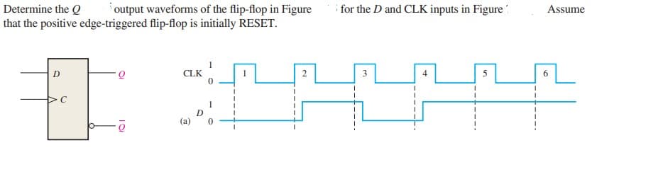
i for the D and CLK inputs in Figure Determine the Q that the positive edge-triggered flip-flop is initially RESET. output waveforms of the flip-flop in Figure Assume D CLK C (a)


Q: Design a modulus seven synchronous counter that can count 0, 3, 5, 7, 9, 11, and 12 using D…
A: A counter is a sequential circuit whose state represents the number of clock pulses fed to the…
Q: Given an AND-gated J-K flip-flop (controlled by raising edge of the clock) as shown. Complete the…
A: Truth-table of given circuit: J1 J2 K1 K2 J K Q 0 0 0 0 0 0 0 0 1 0 1 0 0 0 1 0 1 0 0 0 0…
Q: A flip-flops has a 3 ns delay from the time the clock edge occurs to the time the output is…
A: A flip-flops has a 3 ns delay from the time the clock edge occurs to the time the output is…
Q: 5/ D - Given that the flip flop shown below is initially cleared. A serial input data X= 101100110…
A: Here it is asked to find out the output where input is serially taken. Here D flipflop has been used…
Q: Design a 3-bit Ripple Up-counter Using Negative Edge-triggered Flip Flop
A: Detail solution is in the image
Q: Q2: Draw Block diagram and the Q output from the waveform are applied to the S-R F.F with PRE and…
A:
Q: (4) Consider the following Edge Triggered D Type Flip-Flop with Set (S), Reset (R) and the D inputs.…
A:
Q: Design a counter that counts 0, 1, 2, repeat, using SR flip flops. Show and describe all steps of…
A:
Q: 5. The waveform in Figure Q5 are applied to the inputs of a J-K flip-flops (negative-edge…
A:
Q: (i) Determine how many flip flops are required to build a binary counter that count from 0 to 1023?…
A:
Q: 1-The waveforms in the figure below are triggered D flip flop and a gated D latch (i.e., with enable…
A:
Q: JA JB Kg CLK
A: Here, the flip flop used are J-K flip flop. Write the truth table for J-K flip flop. Inputs…
Q: Experiment 12A. Construct the logic diagram of 4-stage switch-tail ring counter using 4…
A: The Switch tail ring counter or Johnson's ring counter or Twisted ring counter using D flip flop is…
Q: Assume that initially in Figure P9.7. Determine the values of A and B after one Clk pulse. Note that…
A:
Q: Q3) The waveforms in Figure below are applied to the J, K, and clock inputs as indicated. Determine…
A: Truth Table of the JK flip flop
Q: PROCEDURE Draw the circuit diagram of a decade counter using negative edge-triggered flip-flops. The…
A: The truth table for the JK flip-flop is given as: From the above table, It is seen that the output…
Q: Q3) The waveforms in Figure below are applied to the J, K, and clock inputs as indicated. Determine…
A: A JK flip flop Output characteristic Qn+1 = JQ'+K'Q J and K wave form given in figure and let's…
Q: Solve both Draw state diagram of a J-K flip flop. write Verilog code for JK flip flop
A: Flip flop is a latch with additional control input (clock or enable ). A flip flop is used to store…
Q: Design a counter with JK flip-flops that counts primary numbers (2,3,5,7,11,13) in loop, show the…
A: This is a problem of counter design. The solution is shown in the next step
Q: For the input waveforms in figure below, determine the Q output if: 1) The J-K flip-flop is negative…
A:
Q: Please solve both Determine the bit rate if a symbol is represented by 8 bits and the baud is 5000…
A: Latch is asynchronous device. It is level triggered device. It check input and change output…
Q: Figure 1 Explain the difference between D-Latch and D Q3: flip flop with the help of diagram? If the…
A: 3) The difference between D-latch and D Flip flop is as follows: D-Latch : A latch is an electronic…
Q: Determine the Q output for the J-K flip-flop, given .2 tha innuts shown. CLK CLK K K
A: The timing diagram as given in the question gives the states of J, K and the Clock (CLK). Now since…
Q: 4) For the given waveforms determine the output Q and name the reasons for it. assume that the…
A: The given waveform is:
Q: List the binary output at Q for the flip-flop of followed Figure
A: Disclaimer: Since you have asked multiple questions, we will solve the first question for you. If…
Q: JK flip-flops, als olloquially known as jump/kill flip-flops, augment the behaviour of SR…
A: A sequential digital circuit is given. Where initially J=K=0 and C=0, here C is the clock pulse. The…
Q: Design a 2-bit binary counter using: One SR and one JK flip flop.
A: The counter circuit can be designed with the help of state transition table and k map.
Q: Q2: Simplify A PN flip -flop has four operations. clear to zero. no change. complement. and set to…
A: Consider the given data: Here, PN flip-flop operations are, “Clear to 0” for the inputs PN=00 “No…
Q: Q2: Design asynchronous counter to count the sequence 3,4,5,6,7,8,9 and repeat using negative edge…
A: Synchronous counter will have individual clock for each flip flops. Asynchronous counter will have…
Q: Q1) Determine the Q and Q output waveforms of the (D flip-flops) in Figure below. Assume that the…
A:
Q: Design asynchronous MOD-12 counter and draw the timing diagram for each flip-flop output. a.
A: “Since you have asked multiple questions, we will solve the first question for you. If you want any…
Q: Determine the Q output waveforms of the flip-flop in Figure i for the D and CLK inputs in Figure…
A: Latch is asynchronous device. It is level triggered device. It check input and change output…
Q: 8. For the positive-edge triggering JK flip-flop as shown, the waveforms of Q and clock should be:…
A: Given JK flip flop with positive edge triggering shown
Q: Determine the output Q of a positive edge-triggered JK flip-flop for the input waveforms depicted in…
A:
Q: triggered flip-flop) for: (a) T flip-flop with active low clear (CLR') and preset (PRE') (b) T…
A:
Q: 1/0 1/0 d 0/1 0/0 0/0 1/0 1/1 b 0/1 g a 1/1 0/0 0/1 i 0/1 f 0/0 0/0 1/1 h 1/1 0/1 1/1 1/1 1/0
A: As per our guidelines we are supposed to answer only first 3 subparts. Kindly repost the other parts…
Q: 1- Design synchronous counter using negative edge D- type flip flop to count the following states :…
A:
Q: Q2: Determine the Q output waveform if the inputs shown below are applied to a J-K flip flop that is…
A:
Q: Discussion: 1- Design decade counter using D flip flops. 2- Design mod 5 counter using SR flip flop.
A:
Q: (4) Consider the following Edge Triggered D Type Flip-Flop with Set (S), Reset (R) and the D inputs.…
A: The Truth-Table of D type flip-flop is: Clock D Q Q¯ State 0 X Q Q¯ No change 1 X Q Q¯ No…
Q: a) Write the next-state equations for the flip-flops and the output equation. p) Construct the…
A:
Q: Q1: For the J-K flip-flop, determine the Q output for the inputs in figure below Assume that Q…
A:
Q: What is J-K Flip-Flop? Draw it and write its truth .1 table? Determine the Q output for the J-K…
A: As per bartleby we have to solve first question as multiple questions is there .
Q: 2) For the given waveforms determine the output Q and name the reasons for it. assume that the…
A: The given waveform is Use the truth table for D Flip Flop,
Q: Implementation of 8-bit Floating Light Digital Circuit Using JK Flip-Flop design it. (Hint: Using…
A: The implementation of the 8-bit floating light digital circuit using JK flip flop is shown below:
Q: Design a Mode 14 asynchronous forward counter circuit. (Use JK or T type flip-flops) I designed…
A:
Q: Glven a JK fiip-flop, describe thoroughly what the next state Is glven the different Inputs?
A: What is Master-Slave JK Flip Flop? The Master-Slave Flip-Flop is composed of two JK flip-flops…
Q: 3. The waveforms shown in Figure below are applied to a negative edge-triggered JK flip- flop. The…
A: In this question, We need to draw the output waveform of the jK filp flop. We know the output of…
Q: 1) For the given waveforms determine the output Q and name the reasons for it. Assume that the Flip-…
A: The given waveform is:
Q: Determine the output Q for the given J-K flip flop and the waveforms. HIGH PRE J. CLR E LL FFL CL…
A:


Trending now
This is a popular solution!

Step by step
Solved in 2 steps with 1 images

- Flip-flops Give the disadvantages and advantages of Positive Edge Triggering vs Negative Edge Trigerring. Then, give an example of digital circuit and explain where a) Positive Edge is used and b) Negative edge is usedDesign an Implementation of 8-bit Floating Light Digital Circuit Implementation Using D Flip-Flop. Interpret the results. (Hint: Using Shift Register)Design a mod-6 counter with an (active high) enable input E and a maximumcount indicator output Y which is 1 when the counter is at its maximum countand the circuit is enabled. Use JK-FF. In the next-state/output table, please write the state variables in the order Q2Q1Q0. Assume that the unused states will never occur because the flip-flops will be reset on power up, and use don’t cares to simplify the Boolean functions as much as possible.
- Design a sequential circuit with input M and output A using the given state diagram. Reduce the number of states if necessary. Implement the circuit using SR flip-flops. Notes: Use chronological binary assignment for the states (e.g. state A = 0000, B = 0001, D = 0010 etc.) Use Q1, Q2, Q3, Q4 etc. as flip-flop variables where Q1 holds the MSB. Answer the following1. How many SR flip-flops are needed in the design? Note: For numbers 2 to 8 Type N/A if not applicable Use upper case letters, it is case sensitive Use apostrophe to indicate complemented variable For every term in the expression, follow the sequence of the alphabet, e.g., AM’Q1 In case of Q1, Q2, Q3, Q4…, arrange it in ascending order, e.g., Q2’Q42. The input equation to SR flip-flop, SQ1 =3. The input equation to SR flip-flop, RQ1 =4. The input equation to SR flip-flop, SQ2 =5. The input equation to SR flip-flop, RQ2 =6.The input equation to SR flip-flop, SQ3 =7.The input equation to SR flip-flop, RQ3 =8. The output…Sketch a diagram of a 4-bit counter with parallel enable logic that counts down from 15 to 0, then resumes counting down form 15 again. use T flip flops.Design a) a negative edge triggered D Flip-Flop using one active low D-latch and one active high Dlatch. (1st latch is active low; 2nd latch is active high) b) a negative edge triggered D Flip-Flop using one active high D-latch and one active low Dlatch. (1st latch is active high; 2nd latch is active low) c) an active high D latch with enable input C using only NOR gates and inverters.
- For the following statements, write if they are True or False. (a)We can easily build a comparator using XNOR gates. [TRUE/FALSE] (b) Active low decoders can be built with just NAND and NOR gates. [TRUE/FALSE] (c)A “bubble” at the CLK input of a flip-flop means that the flip-flop can be activated by negative-going transitions and level pulses. [TRUE/FALSE] (d)A 3-bit synchronous counter uses an AND gate to reset the output to zero so that recycling can take place. [TRUE/FALSE]A binary pulse counter can be constructed byinterconnecting T-type flip-flops in an appropriatemanner. Assume it is desired to construct a counterwhich can count up to 10010. a. How many flip-flops would be required?b. Sketch the circuit needed to implement this counter.Construct the D-flip-flop with negative-edge triggering using any number of inverters and transmission gates (no asynchronous clearing is needed). The design goal is to minimize the circuit propagation delay from D to Q after the negative clock edge. The circuit inputs are D, CLOCK; there is only one output Q. Show the schematic using inverters and transmission gates as building blocks. Hint: for the Master D-latch output use a complement of Q.
- 12. Aside from Flip Flops being used as a memory, it is also commonly on switches as? 13.For an active low RS FLIP FLOP with a HIGH normal output, the value of its S and R inputs, repectively is ?For the frequency divider circuit the D-flip-flop is a CD4013 Dual D-Type flip-flop V2 is a square wave applied to the Clock input and Q is the ouput waveform. a. What is the frequency of the square wave Clock from V29? b. What is the frequency of the output pin Q? c. How many D-flip-flops are implemented in the CD4013 Chip? d. How many outputs are implemented in each D-flip-flop? List them.2- The following serial data stream is to be generated using a J – K positive edge – triggered Flip – Flop. Determine the inputs required. 101110010010111001000111.