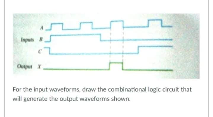
Inputs B Output X For the input waveforms, draw the combinational logic circuit that will generate the output waveforms shown.


Q: By using decoder , design a logic circuit to that can be used as code converter which translate Ex-3…
A: Decimal Number Excess- 3 8-4-2-1 Code w x y z A B C D 0 0 0 0 0 X X X X 1 0 0 0 1 X X X X 2…
Q: Analyze the logic circuits shown below in order to obtain the logic function for each circuit. Write…
A:
Q: draw the logic circuit
A:
Q: Select a suitable example for for combinational logic circuit. O a. None of the given choices O b.…
A: The given questions are from the digital electronics subject. A circuit which remains unaffected by…
Q: For the input waveforms in Figure, what logic circuit will generate the output waveform shown?…
A: Given : Here in the given question they have mentioned the input and output waveforms of a digital…
Q: Determine the output expression of the below logic circuit. A B C F
A: Given, The logic circuit is,
Q: Given a combinational logic circuit whose input is a four-bit number and whose output is the 2's…
A:
Q: Assume that there is a flip-flop with thecharacteristic given in Figure, where A and Bare the inputs…
A: Write the excitation table for the T flip-flop. Flip-flop input Previous state Next state…
Q: Connect the logic circuit and find the output waveform
A:
Q: Q3) Write the Boolean expression for each of the logic eircuits BD-
A: Given data, Two not gate. One OR gate.
Q: What is the main difference between combinational and sequential logic circuits.
A: 1 Combinational Circuit is the circuit in which output is independent of time and only dependent on…
Q: Implement the equation F = ab +ac using a multiplexer and logic gates.
A:
Q: Q2. Minimize the combinational logic circuit in the following figure using Karnaugh's map only.…
A:
Q: Q1. Determine the output waveform and Boolean expression X of the logic circuit in given circuit.
A: Given circuit Y1 is the output of bubbled OR gate Y1=A'+B' Y3 is the output of NAND gate Whose…
Q: It will be designed as a flip-flop synchronous logic circuit with inputs P, N and having the…
A:
Q: Write Verilog code by using structural modeling for the following combinational logic diagram.…
A:
Q: Table 8: Combinational logic circuits Number Parameter Answer As 4.6.1 "AND te 4.6.2
A: 4.6.1 Given combinational logic circuit shown
Q: is it possible to connect the outputs of a comparator to a logic gate (connected to an led)? The led…
A: Steps Let both inputs are low or high at a time and find output of comparator Apply K-Map concept…
Q: (b) Write the Boolean Expression from the given logic circuit in Figure Q5 (B). AD B DC Figure Q5…
A: The solution is as follows.
Q: 2. B. SR Master-Slave Flip-Flop a. Draw the logic diagram of SR master-slave flip-flop and implement…
A: Given, SR master slave flipflop: Y is output of master latch, Q is output of slave latch.
Q: design a logic circuit that accepts decimal input for full adder subtractor circuit with simulation…
A:
Q: Create 8-bit adder/subtractor logic diagram using gates and explain the working of the gates in…
A: Adder is an arithmetic logic circuit designed to add two single bit number with a carry. Truth table…
Q: Q2: Draw a Flowchart to perform the function (G) for the logic circuit shown below, that outputs are…
A: Given
Q: Draw the logic circuit to implement the equation below y : A'BC + B'C' + AB'.
A: To solve above problem one should have basic understanding of AND, OR and NOT gate. For AND gate An…
Q: Minimize the combinational logic circuit in the following figure using Karnaugh's map only.…
A: K-MAP: K-Map is used to optimize the Boolean function by using grouping technique. It's also being…
Q: (i) Write a Boolean expression to represent the output of EACH logic gate. (ii) Next, simplify the…
A: The solution can be achieved as follows.
Q: 6. Draw the circuit that will satisfy this logic equation: - A. B = C
A:
Q: A Write the Boolean expression of the following Logic diagram. BC D= C' 11
A: Given data, Logic diagram
Q: 8) Draw a logic circuit to implement the Boolean function F and with only NOR gates (AC+AB+BC)
A: The function given in question is not in simplified form. To create a logic circuit for given…
Q: 1. Find the minimum output expression for circuit of figure below and draw logic circuit. A
A: In this question we need to minimize the output expression and logic gate.
Q: By using decoder, design a logic circuit to that can be used as code converter which translate Ex-3…
A: Let the Excess-3 code is A,B,C,Dand this excess-3 code is converted into the 8-4-2-1 code which is…
Q: Design a combinational circuit that converts a 4 input binary to gray code... Showing the kmap and…
A: here we have to design a combinational circuit that converts a 4- bit binary to gray code along with…
Q: Draw the logic circuit represented by the following expression. X= A+B[C+ D(B + C)]
A:
Q: Draw the combinational logic circuit diagram by using the equation (ab’ . (a + c))’ + a’b . (a +b’…
A:
Q: Draw the logic circuit for the following function: F = D + BC + (D + C )(A + C)
A:
Q: Draw the logic circuit represented by the following expression. X= A+ B[C+ D(B + C)]
A:
Q: Design a logic circuit using three gates (AND- NAND-OR) that work as an EX-OR gate and write the…
A:
Q: 2. Simplify the logic function f = A+ BC + A(B + C) and draw a schematic for the circuit that…
A: The digital circuits can be combinational as well as sequential circuits. The combinational circuits…
Q: Q2 / Sketch the logic circuit described by the following expression: Y= [ (AB) O (C +B) e D] Z
A: So we need the equivalent logic circuit.
Q: A . В . C X
A:
Q: The sequential logic circuit may include a combinational logic gates circuit True False
A: In this answer we will try to understand whether the given statement is true or false by…
Q: Q6. Draw logic circuit diagram of the Boolean expression. A'B + A(B' + C) + B(B +C').
A: Given:-F=A¯B+A(B¯+C)+B(B+C¯)
Q: Create a synchronous counter utilising J-K flip-flops that may be utilised for a 7-story building's…
A:
Q: (c) Design a synchronous counter using J-K flip-flop that can be used for an elevator system of a…
A:
Q: Design a logic diagram to display a digit 5 using 7-segment display
A: Design a logic diagram to display a digit 5 using 7-segment display ?
Q: Find the output (F) of the logic circuit shown in figure below, for inputs A= 110011 B=010101…
A:
Q: Draw the circuit diagram of a full adder by using two blocks of half-adders and one basic logic…
A:
Q: Select a suitable example for combinational logic circuit. O a. None of the given choices O b.…
A: In this question we need to choose a correct option
Q: Explain, with the help of annotated drawings, the definition and use of noise margins in logic…
A: The noise margins are the amount of noise that an logic circuit can withstand. The value of the…
Q: B) The input waveforms in are applied to logic circuit in figure below. Determine the output…
A:

Step by step
Solved in 2 steps with 1 images

- Design the logic circuit that performs the logic function below. B’(AB+C’)+AGiven the following pullup circuit A-Design the pulldown circuitry B- What is the logic function implemented by this would be?Using Logisim, draw the combinational logic circuit diagram by using the equation: (ab’ . (a + c))’ + a’b . (a +b’ + c’)’
- From the equation A' B C' + A B C D, draw the combinational minimised logic circuit using respective Logic gate symbolsDesign a combinational Logic circuit in which whenever an input is an even number between 1 and 10 a light bulb switches on.Reduce the logic equation with circuit diagram and draw the simplified circuit.
- Given inputs ,AB, and C to hte logic circuit shown, darw hte waveform for the circuit output, Y.Determine the simplified Sum of Product expression of Q1 and Q2 from the table using a K-Map, then draw the simplified logic diagram. SHOW KMAP WITH THE FINAL EXPRESSION & LOGIC DIAGRAMAssume that there is a flip-flop with thecharacteristic given in Figure, where A and Bare the inputs to the flip-flop and Q is the next stateoutput. Using necessary logic gates, make a T flip-flopfrom this flip-flop.