Problem 3 FET Pot-Pourri. Refer to the generic FET figure for this problem. If the substrate doping is NA = 5 x 1016 cm-³, the basic (a) structure is (CMOS, PMOS, NMOS, JFET, MESFET) and the inverted channel charge carriers are (HOLES, ELECTRONS, BOTH HOLES AND ELECTRONS, NEUTRONS, PHOTONS). Metal (or polysilicon) Silicon dioxide (SiO,) G ` If the substrate doping is changed to be Np = 5 x 1016 cm- (b) 3, the basic structure is (CMOS, PMOS, NMOS, JFET, MESFET) and the inverted channel charge carriers are (HOLES, ELECTRONS, BOTH HOLES AND ELECTRONS, NEUTRONS, PHOTONS) Channel region Source region p-type substrate (body) Drain region
Problem 3 FET Pot-Pourri. Refer to the generic FET figure for this problem. If the substrate doping is NA = 5 x 1016 cm-³, the basic (a) structure is (CMOS, PMOS, NMOS, JFET, MESFET) and the inverted channel charge carriers are (HOLES, ELECTRONS, BOTH HOLES AND ELECTRONS, NEUTRONS, PHOTONS). Metal (or polysilicon) Silicon dioxide (SiO,) G ` If the substrate doping is changed to be Np = 5 x 1016 cm- (b) 3, the basic structure is (CMOS, PMOS, NMOS, JFET, MESFET) and the inverted channel charge carriers are (HOLES, ELECTRONS, BOTH HOLES AND ELECTRONS, NEUTRONS, PHOTONS) Channel region Source region p-type substrate (body) Drain region

Introductory Circuit Analysis (13th Edition)
13th Edition
ISBN:9780133923605
Author:Robert L. Boylestad
Publisher:Robert L. Boylestad
Chapter1: Introduction
Section: Chapter Questions
Problem 1P: Visit your local library (at school or home) and describe the extent to which it provides literature...

Related questions
Question
pls write the answers clearly and keep it short so I can follow the steps
thank you
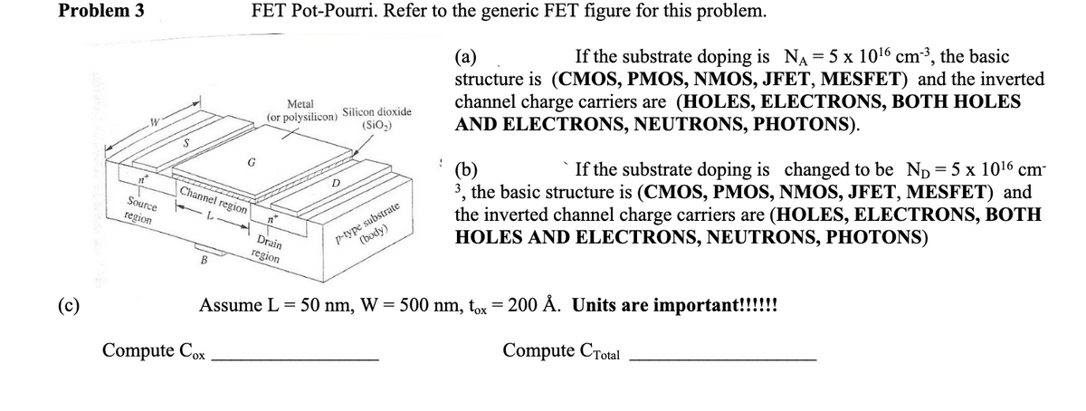
Transcribed Image Text:Problem 3
FET Pot-Pourri. Refer to the generic FET figure for this problem.
If the substrate doping is NA = 5 x 1016 cm³, the basic
(а)
structure is (CMOS, PMOS, NMOS, JFET, MESFET) and the inverted
channel charge carriers are (HOLES, ELECTRONS, BOTH HOLES
AND ELECTRONS, NEUTRONS, PHOTONS).
Metal
(or polysilicon) Silicon dioxide
(SiO,)
G
` If the substrate doping is changed to be Np=5 x 1016 cm-
(b)
3, the basic structure is (CMOS, PMOS, NMOS, JFET, MESFET) and
the inverted channel charge carriers are (HOLES, ELECTRONS, BOTH
HOLES AND ELECTRONS, NEUTRONS, PHOTONS)
Channel region
Source
region
p-type substrate
(body)
Drain
region
Assume L = 50 nm, W =
500 nm, tox = 200 Å. Units are important!!!!!!
Compute Cox
Compute CTotal
Expert Solution
This question has been solved!
Explore an expertly crafted, step-by-step solution for a thorough understanding of key concepts.

Step by step
Solved in 4 steps with 2 images

Knowledge Booster


Learn more about
Need a deep-dive on the concept behind this application? Look no further. Learn more about this topic, electrical-engineering and related others by exploring similar questions and additional content below.Recommended textbooks for you
Introductory Circuit Analysis (13th Edition)
Electrical Engineering
ISBN:
9780133923605
Author:
Robert L. Boylestad
Publisher:
PEARSON

Delmar's Standard Textbook Of Electricity
Electrical Engineering
ISBN:
9781337900348
Author:
Stephen L. Herman
Publisher:
Cengage Learning

Programmable Logic Controllers
Electrical Engineering
ISBN:
9780073373843
Author:
Frank D. Petruzella
Publisher:
McGraw-Hill Education
Introductory Circuit Analysis (13th Edition)
Electrical Engineering
ISBN:
9780133923605
Author:
Robert L. Boylestad
Publisher:
PEARSON
Delmar's Standard Textbook Of Electricity
Electrical Engineering
ISBN:
9781337900348
Author:
Stephen L. Herman
Publisher:
Cengage Learning
Programmable Logic Controllers
Electrical Engineering
ISBN:
9780073373843
Author:
Frank D. Petruzella
Publisher:
McGraw-Hill Education

Fundamentals of Electric Circuits
Electrical Engineering
ISBN:
9780078028229
Author:
Charles K Alexander, Matthew Sadiku
Publisher:
McGraw-Hill Education

Electric Circuits. (11th Edition)
Electrical Engineering
ISBN:
9780134746968
Author:
James W. Nilsson, Susan Riedel
Publisher:
PEARSON

Engineering Electromagnetics
Electrical Engineering
ISBN:
9780078028151
Author:
Hayt, William H. (william Hart), Jr, BUCK, John A.
Publisher:
Mcgraw-hill Education,