Q4. Plot the output waveform Q for a JK Flip-Flop with positive going edge. Does it have any difference if you consider the initial value of Q=1 or Q=0? Clk Clr J
Q4. Plot the output waveform Q for a JK Flip-Flop with positive going edge. Does it have any difference if you consider the initial value of Q=1 or Q=0? Clk Clr J

Chapter22: Sequence Control
Section: Chapter Questions
Problem 6SQ: Draw a symbol for a solid-state logic element AND.

Related questions
Question
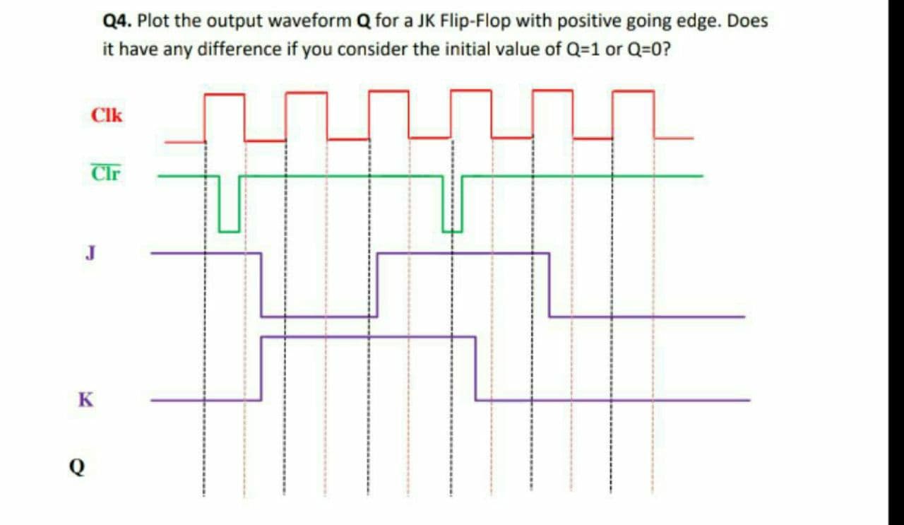
Transcribed Image Text:Q4. Plot the output waveform Q for a JK Flip-Flop with positive going edge. Does
it have any difference if you consider the initial value of Q=1 or Q=0?
Clk
Clr
J
Expert Solution
This question has been solved!
Explore an expertly crafted, step-by-step solution for a thorough understanding of key concepts.

This is a popular solution!

Trending now
This is a popular solution!

Step by step
Solved in 4 steps with 2 images

Knowledge Booster


Learn more about
Need a deep-dive on the concept behind this application? Look no further. Learn more about this topic, electrical-engineering and related others by exploring similar questions and additional content below.Recommended textbooks for you