The half-controlled single-phase bridge circuit shown in : below is supplied at 120 V. Neglecting volt-drops, determine the mean load voltage at firing delay angles of 0°, 60°, 90°, 135°, and 180°. If the load is highly inductive taking 25 A, determine the required device ratings. Find the pf and THD for «=90 is T, 本 Load Z D. Commutating diode Load of resistance with inductai (a)
The half-controlled single-phase bridge circuit shown in : below is supplied at 120 V. Neglecting volt-drops, determine the mean load voltage at firing delay angles of 0°, 60°, 90°, 135°, and 180°. If the load is highly inductive taking 25 A, determine the required device ratings. Find the pf and THD for «=90 is T, 本 Load Z D. Commutating diode Load of resistance with inductai (a)

Power System Analysis and Design (MindTap Course List)
6th Edition
ISBN:9781305632134
Author:J. Duncan Glover, Thomas Overbye, Mulukutla S. Sarma
Publisher:J. Duncan Glover, Thomas Overbye, Mulukutla S. Sarma
Chapter2: Fundamentals
Section: Chapter Questions
Problem 2.52P: A balanced three-phase load is connected to a 4.16-kV, three-phase, fourwire, grounded-wye dedicated...

Related questions
Question
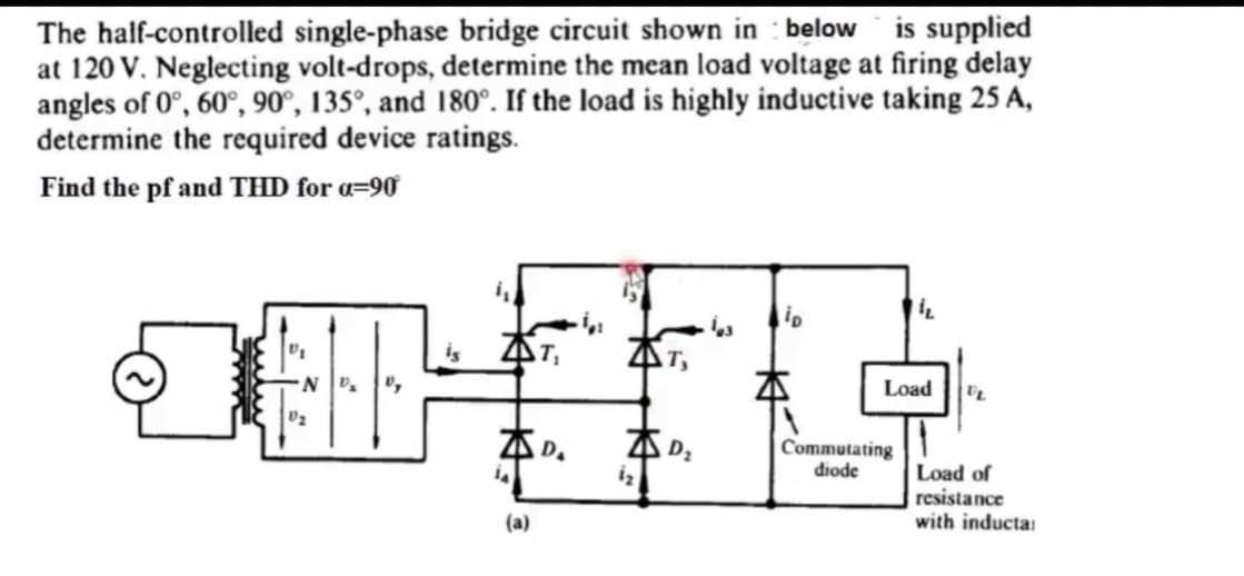
Transcribed Image Text:The half-controlled single-phase bridge circuit shown in : below is supplied
at 120 V. Neglecting volt-drops, determine the mean load voltage at firing delay
angles of 0°, 60°, 90°, 135°, and 180°. If the load is highly inductive taking 25 A,
determine the required device ratings.
Find the pf and THD for «=90
is
AT,
T,
Load
ZD.
Commutating
diode
Load of
resistance
with inductai
(a)
Expert Solution
This question has been solved!
Explore an expertly crafted, step-by-step solution for a thorough understanding of key concepts.

Step by step
Solved in 2 steps with 2 images

Recommended textbooks for you
Power System Analysis and Design (MindTap Course …
Electrical Engineering
ISBN:
9781305632134
Author:
J. Duncan Glover, Thomas Overbye, Mulukutla S. Sarma
Publisher:
Cengage Learning
Power System Analysis and Design (MindTap Course …
Electrical Engineering
ISBN:
9781305632134
Author:
J. Duncan Glover, Thomas Overbye, Mulukutla S. Sarma
Publisher:
Cengage Learning