
Computer Networking: A Top-Down Approach (7th Edition)
7th Edition
ISBN: 9780133594140
Author: James Kurose, Keith Ross
Publisher: PEARSON
expand_more
expand_more
format_list_bulleted
Related questions
Question
Can someone explain the process of the diagram? I am not looking for a particular answer, I just want simple definitions about some of the main components' function... also, sequence or direction of this diagram
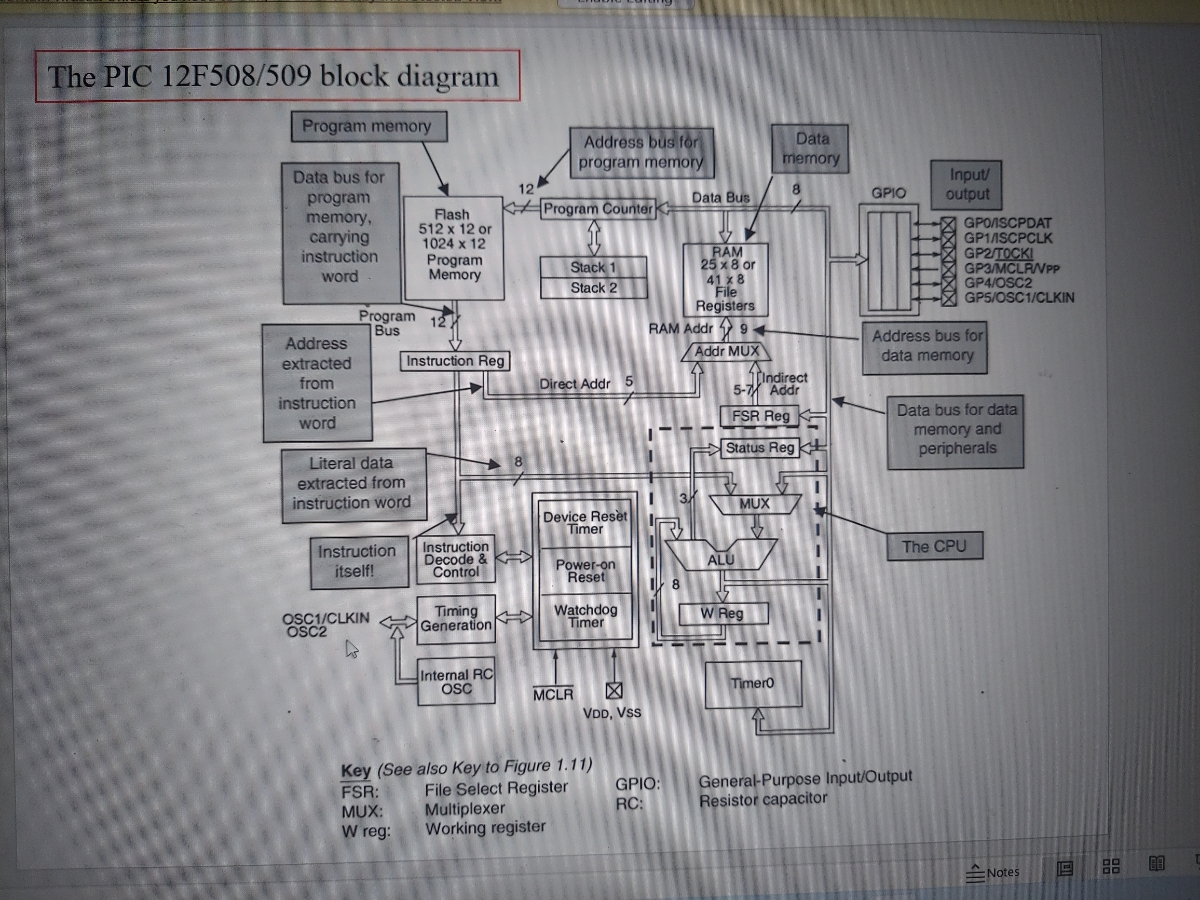

Transcribed Image Text:The PIC 12F508/509 block diagram
Program memory
Data bus for
program
memory,
carrying
instruction
word
Address
extracted
from
instruction
word
Program 12
Bus
Literal data
extracted from
instruction word
Instruction
itself!
Flash
512 x 12 or
1024 x 12
OSC1/CLKIN
OSC2
4
Program
Memory
Instruction Reg
Instruction
Decode &
Control
Timing
Generation
Internal RC
OSC
124
Program Counter
Address bus for
program memory
Stack 1
Stack 2
Direct Addr 5
Device Reset
Timer
Multiplexer
W reg: Working register
Power-on
Reset
MCLR
Watchdog
Timer
VDD, VSS
Key (See also Key to Figure 1.11)
FSR:
File Select Register
MUX:
IT
RAM Addr 9
Addr MUX
3
R₂
GPIO:
RC:
Data Bus
8
V
RAM
25 x 8 or
41x8
File
Registers
ALU
5-7 Addr
FSR Reg
Status Reg
MUX
V
W Reg
Data
memory
Indirect
8
Timero
GPIO
Input/
output
GPO/SCPDAT
GP1/SCPCLK
GP2/TOCK!
GP3/MCLR/VPP
GP4/OSC2
GP5/OSC1/CLKIN
Address bus for
data memory
Data bus for data
memory and
peripherals
General-Purpose Input/Output
Resistor capacitor
The CPU
: Notes
DO
80
Expert Solution
arrow_forward
Step 1
Functions of peripherals (PIC12F508/509):
• 6 I/O pins:
- 5 I/O pins with individual direction control
- 1 pin for input only
- High voltage sink/source for direct LED power
- Wake-on-change
- Weak strokes
• 8-bit real-time clock/counter (TMR0) with 8-bit
Programmable pre-divider

Step by stepSolved in 3 steps

Knowledge Booster

Similar questions
- It is essential to explain the differences between Diagrams 0 and 1. Exists in the Context diagram any symbols that are not being utilised?arrow_forwardFor a variable to be fully defined, its type and any other information it may have must be provided (and therefore complete). All variables, in another way of putting it, have not just a data type but also other qualities. To better describe the characteristics of each variable we encounter, please elaborate on the idea that will help us do so.arrow_forwardExplain what Systems Dynamics is all about using your own words by way of explanation. also Provide an explanation of a reinforcing loop using your own words as an example. Which fundamental equations serve as the foundation for systems dynamics?arrow_forward
Recommended textbooks for you
- Computer Networking: A Top-Down Approach (7th Edi...Computer EngineeringISBN:9780133594140Author:James Kurose, Keith RossPublisher:PEARSON
 Computer Organization and Design MIPS Edition, Fi...Computer EngineeringISBN:9780124077263Author:David A. Patterson, John L. HennessyPublisher:Elsevier Science
 Network+ Guide to Networks (MindTap Course List)Computer EngineeringISBN:9781337569330Author:Jill West, Tamara Dean, Jean AndrewsPublisher:Cengage Learning
  Concepts of Database ManagementComputer EngineeringISBN:9781337093422Author:Joy L. Starks, Philip J. Pratt, Mary Z. LastPublisher:Cengage Learning
 Prelude to ProgrammingComputer EngineeringISBN:9780133750423Author:VENIT, StewartPublisher:Pearson Education
 Sc Business Data Communications and Networking, T...Computer EngineeringISBN:9781119368830Author:FITZGERALDPublisher:WILEY
Computer Networking: A Top-Down Approach (7th Edi...
Computer Engineering
ISBN:9780133594140
Author:James Kurose, Keith Ross
Publisher:PEARSON
Computer Organization and Design MIPS Edition, Fi...
Computer Engineering
ISBN:9780124077263
Author:David A. Patterson, John L. Hennessy
Publisher:Elsevier Science
Network+ Guide to Networks (MindTap Course List)
Computer Engineering
ISBN:9781337569330
Author:Jill West, Tamara Dean, Jean Andrews
Publisher:Cengage Learning
Concepts of Database Management
Computer Engineering
ISBN:9781337093422
Author:Joy L. Starks, Philip J. Pratt, Mary Z. Last
Publisher:Cengage Learning
Prelude to Programming
Computer Engineering
ISBN:9780133750423
Author:VENIT, Stewart
Publisher:Pearson Education
Sc Business Data Communications and Networking, T...
Computer Engineering
ISBN:9781119368830
Author:FITZGERALD
Publisher:WILEY