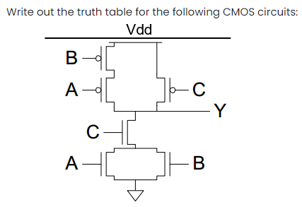
Write out the truth table for the following CMOS circuits: Vdd B- A- -Y C- A-


Q: 3. Define Tri-State TTL gate. Write down the three output states of Tri-State gate. Also draw the…
A:
Q: Q. 7 Implement the function f = (x1 + x2X3)(x4) using CMOS network.
A: CMOS network
Q: This guestion considers the logic function f(a,b,c,d) = (a+b+c)•d. %3D (a) Design and draw a custom…
A: The logic function is given below, fa,b,c,d = a+b+c·d¯
Q: Question 4.Do a research and find the answers for the following questions 1. Find the diagram image…
A:
Q: is CMOS static Logic circuits tree. Explain each item with supporting diagrams and give their…
A:
Q: Design CMOS Layout for the Boolean function Y=A[(BC)+D].
A: Consider the given function as, Y=A[(BC)+D]
Q: Sketch a schematic for the two-input XOR function using only NAND gates. How few can you use?
A: We are authorized to answer one question at a time, since you have not mentioned which question you…
Q: Write an HDL gate-level description of the circuit shown in
A:
Q: A CMOS source can properly drive ___ LSTTL gates without exceeding its drive capabilities a) 0 b)…
A: CMOS:- It is the combination of PMOS and NMOS transistors. CMOS semiconductor dissipates low power…
Q: Implement the function f = (x1X3 + x2)(x4) using CMOS network. %3D
A:
Q: Find VH for an NMOS logic gate with a saturatedload if VT O = 0.75 V, γ = 0.75 √V, 2φF = 0.7 V,and…
A: Given data: VTO is: 0.75 V VDD is: 3.0 V The expression for the VH is given as, The expression for…
Q: (d) Draw the folowing Boolean expression using CMOS transistors. (i) Y = AD + AE + BC. (ii) Y = ACD…
A:
Q: You have been asked to design an intruder alarm circuit using logic gates. Compare TTL and CMOS…
A: Intoduction - TTL technologies - TTL is an abbreviation for Transistor-Transistor Logic. Every logic…
Q: A B Output (F) 1 1 1 1 1 1 1 1 1 1 1 1 1 1
A: Given:We need to satisfy the given table using CMOS logic: where a clear logic is given and inputs…
Q: HW: (a) Design a CMOS logic circuit that implements the logic function. f(A,B,C) = A + BC
A: Since you have posted multiple questions, we will solve the first question for you. If you require…
Q: Problem 2. The following diagram shows a schematic for the pullup circuitry for a particular CMOS…
A: (A) the schematic for the pulldown circuitry for this CMOS gate is shown below,
Q: Implement the following functions using dynamic CMOS logic. Further, comment on the number of…
A:
Q: integrated circuit families (RTL, DTL, TTL, CMOS) 4. Let vx = vy = 0.1V (Logic 0), B = 25 Determine…
A:
Q: Calculate the number of transistors required toimplement a 8-bit column decoder using (a)NMOS…
A: a) Calculating number of transistor required to implement a 8-bit column decoder using NMOS…
Q: Q5: Explain the construction, operation, characteristic tables and timing d following sequential…
A:
Q: Provide a CMOS realization of the following negative logic gate. The negative logic truth table and…
A: CMOS is define as the semiconductor device which are used in fabrication of integrated chips.
Q: CMOS is famous because it has a high noise immunity? Select one: True O False
A: We are authorized to answer only 1 question at a time since you have not mentioned which question…
Q: Find VH for an NMOS logic gate with a saturatedload if VT O = 0.6 V, γ = 0.6√V, 2φF = 0.6 V,and VDD…
A: Given data: VTO=0.6 Vγ=0.6VVDD=3.3 V The expression for the VH is given as, VH=VDD-VTNL The…
Q: The following digital IC is: TTL AND gate OTTL NOT gate CMOS NAND gate TTL NAND gate OCMOS AND gate…
A: Given, Digital IC (integrated Chip ) is SN 7400 N
Q: 4 Sketch HI-skew and LO-skew 4-input NAND and NOR gates. What are the logical efforts of each gate…
A:
Q: Use the following space to draw the pull-down and pull-up graphs of a static CMOS complex gate…
A: The following figure is the CMOS equivalent network of the given boolean expression:
Q: A certain gate draws 2 mA when its output is HIGH and 5 mA when its output is LOW and transition…
A: Given thatGates draws 2mA when its output high.5mA when its output lowIccH transition time 3mA…
Q: Satisfy the given table with three inputs using CMOS Logic. Write a clear logic diagram and label…
A:
Q: What are the worst-case rise and fall times andaverage propagation delays of the CMOS gate inFig.…
A: (b) In worst case, Two NMOS are in series The width to length ratio is given as,…
Q: CMOS 3 INPUT NOR GATE FOR PULL UP AND PULL DOWN NETWORKS
A: CMOS 3 INPUT NOR GATE FOR PULL UP AND PULL DOWN NETWORKS
Q: 2. Build CMOS circuit using Bubble Pushing & Structure method: a) F = (a + b)(c + d) b) F = ab + cd…
A: We need to design the given Boolean function by using CMOS gate .
Q: Q4: Wright the Intermediate Circuit Description Language (ICDL) of the CMOS 3- inputNAND gate.…
A: BJT and MOSFET are the class of transistors used in analog electronics. They are widely used…
Q: integrated circuit families (RTL, DTL, TTL, CMOS) 4. Let vx = vy = 0.1V (Logic 0), B = 25 Determine…
A:
Q: Q4: Wright the Intermediate Circuit Description Language (ICDL) of the CMOS 3- inputNAND gate.…
A: BJT and MOSFET are the class of transistors used in analog electronics. They are widely used…
Q: Q7//Design 4-bit binary to gray conversion using read only memory.
A:
Q: Vdd Y A- B- C- D-
A:
Q: b) How are the two levels of the clock defined in clocked CMOS ckt? Draw the circuit of Clocked CMOS…
A: According to the question, we need to discuss the two levels of the clock defined in the clocked…
Q: Obtain the logical network function of the following n CMOS gates. Out
A: A MOSFET is a three-terminal device in which the source-drain conductance can be controlled by the…
Q: Design the CMOS diagram for the following Table: (A, B & C are the inputs and Y is the output in the…
A: We have to design the cmos diagram
Q: Design complex CMOS logic gates.
A: The complex CMOS logic gate is as follows:
Q: How many NFETS is needed to implement the following function with a single CMOS gate (F-6C+AD):…
A:
Q: Draw the following logic function using CMOS logic: F = A.B' .(C+D'.E)+F' 4:07 PM
A: I seperately showed the complement or NOT of a variable and for others also you need to use in…
Q: a) For the logic function f a. (b + c), using CMOS concept draw the stick diagram and write the pull…
A: Here we need to design the given logic function using CMOS. The generalized block diagram will be
Q: What are the status of the following CMOS gates when both inputs A and B are 1s? V DD P1 A P2 B Y
A:
Q: i) Construct a CMOS NAND gate, NMOS NAND gate and NMOS NOR gate. ii) What are the differences…
A: We need to construct a CMOS Nand gate Nmos Nand gate and NMOS nor gate.
Q: Using MOSFETs, implement the following Logic Function: f = AB'+C+D
A: Given: Logic Function: f = AB'+C+D We have to design using above circuit using MOSFETs.


Trending now
This is a popular solution!

Step by step
Solved in 2 steps with 2 images


- Construct a Truth Table on the Following CMOS Circuit. answer only this question please : Implement the function f using CMOS network.Digital Electronics and Design Questiona) Find the logic function ‘F’ realized by the CMOS circuit below. b) Complete the missing logic signals in the circuit. c) Write the Verilog HDL or VHDL code that implements the logic function.
- build CMOS circuits (using truth-table method) for both of the functions.**this is for introduction to VLSI course**Make a truth table for the CMOS circuit.A certain packaged IC chip can dissipate 5W. Supposewe have a CMOSIC design that must fit on onechip and requires 10 million logic gates. What is theaverage power that can be dissipated by each logicgate on the chip? If the average gate must switch at100 MHz, what is the maximum capacitive load ona gate for VDD =3.3 V, 2.5 V and 1.8 V.
- Design a CMOS gate circuit for the Boolean expression (circuits and inputoutput curves) on PspiceF= XZ+ XYW(where W, X, Y and Z are inputs)Use three MSI circuits,construct a binary parallel adder to add 12 bit binary numbers. Label all carries between the MSI circuit.TOPIC: COMBINATIONAL CIRCUIT What is a half-adder? Write its truth table. Design a half-adder using NOR gates only. What is a full-adder? Draw its logic diagram with basic gates. Implement a full-adder circuit using NAND gates only. Implement a full-adder circuit using NOR gates only. What is a multiplexer? How is it different from a decoder? How are multiplexers are useful in developing combinational circuits? What are the major applications of multiplexers?
- Satisfy the given table with three inputs using CMOS Logic. Write a clear logic diagram and label the inputs properly.Using four MSI circuits, construct a binary parallel adder to add two 16-bit binary numbers. Label all carries between the MSI circuitThe number of PMOS transistors required to implement 3-input Nand Gate using Dynamic CMOS logic: a. 5 b. 1 c. 6 d. 4