1. Determine in which mode (depletion, enhancement or neither) each D-MOSFET in the figure -Vpp below. +Vpp +VpD Rp +VpD Rp Rp Rp Rs Ro RG Rs RG (d) (b) (a)
Q: 100 V battery voltage to 75 V need a da-da circuit to reduce the voltage is heard. Transducer…
A: Part (a): Since the output voltage is less than the input voltage, a step-down converter is used. A…
Q: IV) Explain the operating principle of a dual-slope ADC circuit, in your own words
A: ADC (ANALOG TO DIGITAL CONVERTER)- It converts analog signals to digital signals. ADC signals are of…
Q: Unit 4 During tum-on and tum-off of a power transistor, the -Vx current-time and voltage-time…
A: “Since you have asked multiple questions, we will solve the first question for you. If youwant any…
Q: For the Common Base circuit given in Figure 2 , draw the DC load line and locate its 1 and neglect…
A: Redraw the circuit , When the transistor is given the bias but no signal is applied at its input…
Q: Q OUT CLK
A: STATE TABLE OF D-FLIP FLOP: D(Input) Qn+1(Next sate) 0 0 1 1 CHARACTERISTICS TABLE OF…
Q: 3. Write down which transistor structure each curve characteristic belongs to in the figure. VGs…
A:
Q: What are the output current and output resistance of the current source as shown if VDD = 10 V, R4 =…
A:
Q: Q1. In the circuit Figure 1, ß is in range 75 < p s150 , Determine the range in (a) Small signal…
A:
Q: Calculate the maximum load current ILmax in mA if E=12V, R=170 ohm, that will ensure that the…
A: We need to find out maximum load current for given voltage regulator .
Q: What is the Q-point of the transistor ifR1 = 470 kΩ, R2 = ∞, R3 = 27 kΩ, R4 = 51 kΩ,and VDD = 12…
A: Calculating gate to source voltage
Q: Calculate the drain current ID and the source drain voltage VDS. R1 = 15kohms, R2 = 15kohms, RD =…
A:
Q: c. Draw the d.c load line for the circuit diagram shown below. What will be the Q point if zero…
A: Given circuit can be drawn as zero signal-- Short circuit IB=25μAβ=60IC=βIB=25×60μA…
Q: Draw small signal equivalent circuit and derive expression of voltage gain RD R Vo Cc R2 Rs -5 V ww…
A: MOSFET(Metal Oxide Semiconductor field effect Transistor) is three terminal electronic device.…
Q: For the given circuit; >Setup state transition table D (J >Sketch state transition 2x1 diagram…
A:
Q: Find the Q-point for the transistor for R1 = 100 kΩ, R2 = 220 kΩ, R3 = 24 kΩ,R4 = 12 kΩ, and VDD…
A:
Q: The four-resistor bias network of Figure12.22(a) on page 620 has VCC = 15 V, R1 = 100 kΩ, R2 = 47…
A: In self-basing circuit, the equivalent voltage (VS) and the resistance at base terminal are given:…
Q: For the transistor in Figure P5.38, B = 80. Determine the range in V1 that produces 3 < VCEQ<9 V.…
A:
Q: 5. For the circuit shown in Figure C3 a. Draw the DC load line in the Graph C3 D. Calculate the Q…
A:
Q: For the circuit, take VTN=0.8V, the conduction parameter Kn-1 mA/V2 and X-0. Calculate the…
A:
Q: Identify the source, drain, gate, and bulk terminalsand find the current I in the transistorsAssume…
A: The labelling for NMOS transistot is as follows
Q: As a maintenance engineer in a semiconductor company, you are given a task to replace the current…
A: i) ID=41×103=4mAVD=16-1.8KID =16-1.8K×4mA =8.8VVG=1.2K1.2K+3.6K×16 =4VVGS=4-4=0V
Q: A voltage divider-bias circuit N-channel Junction Field Effect Transistor (JFET) shown in Figure…
A:
Q: (CLO-3, C3, C5 , C4) a. Draw a Thevenin equivalent circuit of the circuit shown in the figure below…
A: This is a very simple question based on voltage divider bias . In this all the 3 steps are described…
Q: What is the value of tP0 for a technology with L = 250 nm, n = 500 cm2/V-s,VDD = 3.3 V and VT N =…
A: Concept: The two expressions connected by equal to be called an equation. The expression on the two…
Q: 10 In the circuit shown in Figure P11.10, a drain voltage of 0.1 V is established. Find the current…
A: Given data: vGS=15 VVT=1 V Calculating vDS, vDS=vD-vS=0.1-0=0.1 V
Q: (ß = 100, V¼ = o, Vr = 25mV,Ic = 1.7 mA) a) Draw small signal equivalent circuit. b) Calculate Rin :…
A: “Since you have posted a question with multiple sub-parts, we will solve the first three subparts…
Q: Draw ac equivalent circuits for the following amplifiers. Each circuit should include resistances…
A: According to company guidelines, only the first 3 subparts will be solved. If another subpart is…
Q: Consider the circuit shown in Figure P3.33. The transistor parameters are VTN = 0.4 V and k, = 120…
A:
Q: Calculate the drain current of the MOSFET circuit below: VDD Vop = 6V %3D - Vap = -6V vo RD Ri= Rz=…
A:
Q: Q3) For the shown figure below ,Assume VTN =1 V, VTp =-1 V,and Kn =Kp =2 mV/V?. a)Calculate Ip and…
A: Given circuit is shown below. Given data is a) if PMOS will be OFF for , NMOS will be OFF for .…
Q: Figure 4 shows the transfer curve of a network with an unknown channel Junction Field Effect…
A: Given: Required: (1) Identify the channel of JFET and justify the answer. (2)…
Q: Determine Rout for the Common Source E-MOSFET circuit in the figure. Assume this particular MOSFET…
A:
Q: 7. MOSFET circuit The MOSFET in the circuit below has V = 1 V and kn = 4 mA/V². a) Is the MOSFET…
A:
Q: A. A voltage regulator circuit provides a constant voltage of (6 V) across a load resistance of (2…
A: Given: Load resistance, RL=2kΩ Minimum current required for Zener operation, Izmin=5mA Maximum…
Q: (c) For the circuit in Figure Q4 (c) with +Vcc=39 V, -VEE = - 39 V, RL = 8.8 N, calculate: (i) Input…
A: The given circuit is a Class B power amplifier and the required parameters can be analyzed with the…
Q: Q2) An npn transistor circuit as shown in figure below has a = 0.985 and VBE = 0.3V. If Vcc=16V,…
A: From given current gain alpha calculate collector current and emitter current. Now applying KVL…
Q: 1) Design the bias of MOSFET such that the Q-point is in middle of saturation region. ssume Vtn =lv,…
A:
Q: V-SV Figure 3 Calculate the small-signal parameters gam, Fn, and ro. Draw the small-signal…
A:
Q: Example 1: For the circuit shown in Figure 4 () Draw the DC load line (ii) Calculate the Q point if…
A: Given data: VCC=10 V R1=2500 Ω α=0.975 IB=50 μA (i) Load line can be drawn by using the below…
Q: Given a voltage divider configuration of a D-MOSFET with IDSS = 12mA, VP = -3V, yos = 35µS, R1 =…
A: “Since you have posted a question with multiple sub-parts, we will solve first three subparts for…
Q: JESTION 6: Consider the circuit of Figure P11.3 with transistor parameters ß = 155 , V4=∞, and…
A:
Q: Consider the circuit shown if Figure (Q2). Design this circuit such that the drain current is 0.1 mA…
A:
Q: Q1. Assume BDC = 150, VCE(sat) = 0 V and IC(cut off) = 0 A. (a) Let VBB = 10 V, determine the…
A:
Q: What is the effect of increasing resistor R2, in the voltage-divider bias circuit on ICQ? How should…
A: The base voltage across R2 is voltage divider bias voltage where, VR2=VCC.R2R2+R3 To increase the…
Q: In the following figure, Q1 and Q2 are identical and operate in active mode. if Ic1 = 12 Ic2 then…
A: IC1 = collector current of transistor Q1 IC2 = collector current of transistor Q2. V1 = forward…
Q: 5.46 Consider the circuit in Figure P5.46. For the transistor, B = 50. Find Is,lc. Ig, and Vo for…
A:
Q: In the transfer characteristics shown below in Figure A, Vth is: [Approximate time to answer: 2…
A: we need to find out Vth.
Q: Figure Q4a shows a basic current mirror structure (in its 'sink' form) which is designed to provide…
A: IR =IC1+2IB IB1=IB2=IBIC2 = IoIB2=Ioβ IC1 = βIB1 = βIoβ=Io
Q: (iii) What is meant by drain characteristics (b) Determine the drain current of an n-channel JFET…
A:
Determine in which mode (depletion, enhancement or neither) each D-MOSFET in the figure below.
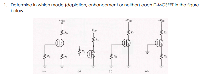
Trending now
This is a popular solution!
Step by step
Solved in 2 steps with 2 images
- 6. Through the schematic symbols of MOSFETS, how can you differentiate between a depletion and an enhancement type MOSFET? P-channel or N-channel MOSFET?How do we know current flows in source terminal? Is this common for n-type mosfet? What is an n-type mosfet?Describe the operation of an n and a p type enhancement and depletion mode MOSFET
- In your own words, briefly describe the basic operation of an E-MOSFET.Suppose -Vcc is connected to the ground, What happens to the LED when Vin< Vref and how? What is the use of RL here and how is its value computed? Should the Vout also be connected to the ground?Draw the load line for the circuit given in figure-1 and also calculate the saturated collector current and VCEat half cut-offpoint?
- Explain the concept of a very large-scale integrated circuit (VLSI).5. In your own words, briefly describe the difference between the basic operation of a pchannel depletion-type MOSFET and p-channel Enhancement-type MOSFET.What is the role of resistor R3 in getting the low bias current we are obtaining out of the Widlar source? I don't really know the importance of R3 when looking at the figure. Is it because it controls the amount of current flowing through the transistor?
- Explain the concept of power semiconductor devices such as Insulated Gate Bipolar Transistors (IGBTs) and Thyristors. How do these devices enable efficient power control and switching in high-power applications?Draw the block diagram of a HVDC converter station and briefly describe the function of each Component.Define LCC and VSC and compare their performancedraw a qpsk modulator circuit using different circuit compents like resistors, transistors etc not a block diagram