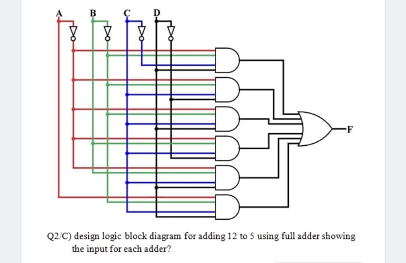
B F Q2/C) design logic block diagram for adding 12 to 5 using full adder showing the input for each adder? Do
Q: draw the logic diagram of 4x1 Multiplexer below (with depicting the internal structures). Indicate…
A: A simple problem on digital electronics. Look below for solution:-
Q: 3. Define Tri-State TTL gate. Write down the three output states of Tri-State gate. Also draw the…
A:
Q: Q5. Design a decoder to convert the 421 BCD codes to drive a 7-segment LEDS that displays the…
A:
Q: Q1/ Draw the logic circuit after simplify the circuit show below using K. map: B Y
A: First we will convert the above circuit into its POS form which is Y=A+B+C·A+B+C·A+B+C
Q: ülebäi The logic circuit represented by the figure shown below is A Doz B OR O AND O NAND O NOR O
A:
Q: Distinguish between Half Adder and Full Adder as applied in combinational logic circuit
A: In digital electronics circuit are classified in two categories: Combinational circuit Sequential…
Q: Logic gate No. 4 * B D F4 E
A:
Q: Q11:design a two input logic circuit (A, B) to implement And, Or,Xor,Complement using Mux and logic…
A: As per company guidelines we are supposed to answer only one question. Kindly repost other questions…
Q: is CMOS static Logic circuits tree. Explain each item with supporting diagrams and give their…
A:
Q: 16) For the circuit that is shown in the Figure shown below. LG represent logic circuit with the
A: Given values are: X1=0,X2=1,X3=1,X4=1,X5=1. And output after function passing through LG is given…
Q: Distinguish between Half Adder and Full Adder
A: Adder: Adder is digital circuit that performs addition operation of numbers. In computers adders…
Q: Q2. Minimize the combinational logic circuit in the following figure using Karnaugh's map only.…
A:
Q: Q2:Draw the logic circuit to Storage the data (110110).
A: As per the guideline we need to solve only first question. we need to draw the logic circuit to…
Q: Figure Q.4 (a) shows a combinational logic circuit with output, Z and Table Q.4(a) depicts the delay…
A: According to the question, for the figure shown below We need to find the critical path and…
Q: i. Design full adder using two half adders. ii. Draw the circuit diagram of 4-bit Ripple Carry…
A:
Q: Design a digital logic circuit designing various circoits to compute the 9 5 compliment of a binary…
A: Thank you for the question as per the company policy I will be solving first three sub-parts of the…
Q: Design and draw the logic diagram for a two-input NAND gate using one two-input AND and one NOT…
A:
Q: logic gate circuit diagram and truth table for F=AC(B+D) +BD(A+C)
A:
Q: Implement a 2 bit Full Adder in product of sums and Draw logic circuit diagram
A:
Q: Q1 Figure Q1 depicts a simple combinational logic circuit. Give: (a) the VHDL entity and (b) a…
A:
Q: 2. B. SR Master-Slave Flip-Flop a. Draw the logic diagram of SR master-slave flip-flop and implement…
A: Given, SR master slave flipflop: Y is output of master latch, Q is output of slave latch.
Q: Create 8-bit adder/subtractor logic diagram using gates and explain the working of the gates in…
A: Adder is an arithmetic logic circuit designed to add two single bit number with a carry. Truth table…
Q: ii. Draw logic diagram of half subtractor.
A:
Q: Example: 4 A bit asynchronous binary counter is shown in the Figure. Each flip-flop is negative…
A: Here it gives 4 bit assynchronous counter of JK flip flop here gives negative edge triggered timing…
Q: Draw the logic circuit for (a'+ b'+ c + d) (a+ b+ c'+ d) (a+ b'+ c +d) using NOR gates.
A: The solution is as follows.
Q: logic circuit diagram for fabinaaci counter that gives output in fabinaaci sequence
A: Combinational logic circuit is a circuit whose input is dependent on the output,
Q: Minimize the combinational logic circuit in the following figure using Karnaugh's map only.…
A: K-MAP: K-Map is used to optimize the Boolean function by using grouping technique. It's also being…
Q: Draw and explain the logic diagram for frequency divider (Use 3 J-K flip-flops and assume 32 kHz…
A:
Q: A logic gate that will give a high output if all the inputs are low, and a low output if any one of…
A: According to the given question there exist a logic gate which will which will produce output high…
Q: A B Ca D 2 -2
A: In order to implement nmos two input AND logic it takes 3 Nmos . Nmos implementation for two input…
Q: Problem / Draw each expression the logic gate 1 X = ABC + ABC + ABC + ABE @ X= (A+B) (C+D) (E+F) (3)…
A:
Q: Draw in Table 3 the circuit schematic of each segment using the basic logic gates in kmap
A: According to the given question, The logic diagram of the above-given SOP equation can be drawn by…
Q: 1. Find the minimum output expression for circuit of figure below and draw logic circuit. A
A: In this question we need to minimize the output expression and logic gate.
Q: (d) For the decimal to BCD encoder logic of the following circuit, assume that the 9 input and the 3…
A: There are multiple independent questions. As per the guidelines we can solve one question at a time.…
Q: Design the circuit of OR gate with three input by using simple logic module ?
A:
Q: 3.Draw the logic diagram of a 5-bit parallel binary adder using a combinationof half adders and full…
A: 5-bit parallel binary adder using half adder (HA) and full adders (FA) :
Q: Design the circuit of OR gate with three input using simple logic module ?
A: Given that: The number of inputs =3 Output =1
Q: Write a VHDL code for the following simple logic circuit. X1 X2 f X3
A:
Q: Q3) Design a 4-bit even parity generator circuit using: а. Basic logic gates. b. Decoder IC.
A: As per our guidelines we are supposed to answer only one question. Kindly repost other questions as…
Q: For the logic diagram shown in Figure Q23 prove it is working as Ex-OR gate.
A:
Q: A . В . C X
A:
Q: Logic gate No. 1* A E B D
A:
Q: 9. Analysis of Synchronous Counters, in the following figure, write the logic equation for each…
A:
Q: : Describe any two Digital Logic Gate with its truth table and high light it properties
A:
Step by step
Solved in 3 steps with 3 images
- draw the logic diagram using three basic 2-input logic gates F=(A'+C) (A'+ C') (A+B+C'D)logic circuit diagram for fabinaaci counter that gives output in fabinaaci sequence.upto 2 digits please mentions the gates and ics used in circuit.Draw a 14 ic chip wiring diagram with labeled switches(A, B, C) of a 3 input of this logic diagram.
- Provide the correct answer and write a legible solution. 1. Simplify the expression G = (X’ + Y + Z’) (W + X + Y + Z) (W’ + X’ + Y’) using K- map and draw the corresponding simplified logic gate circuit.Digital Logic Design Show the Diagrams, please as well. Must answer according to the Questions exactly.subject: Digital Logic &Design Q: Describe the operation of a basic parity generating and checking logic
- Figure 4 shows the decimal to BCD encoder logic. Assume that the 9 input and 3 inputare both HIGH.i) Determine the output code.ii) Is the value valid for BCD (8421) code?We want to design a circuit to detect prime numbers.The input of the circuit is a 4-bit binary number and the output is a single bit and should show one when the number is prime and zero otherwise.B. Implement the circuit using a 4× 1 multiplexer and combinational logic gates.C. Implement the circuit using only one decoder and one OR gate. What is the size of the decoder you use?Find a logic diagram that corresponds to the VHDL structural description in below figure. Note that complemented inputs are not available
- Draw logic diagram for half adder and full adder circuit using Logisim Software5) below is the accuracy table showing the output values for two separate binary number entries (W and Y) with a length of two bits. Get the simplest form of output functions with the Karnaugh diagram. Draw a logic diagram of the circuit that performs the function of these functions.Describe in detail which functions a, b and C perform for 2-bit binary numbers in the input.Use the equivalent NAND gate logic to convert the logic diagram in Figure 5.1 below to only contain NAND gates. Redraw the logic diagram with input/output labels.