
Concept explainers
Videos
The two possible situations that will happen for the given conditions.
The diode current and terminal voltage across diode for two situations.
Answer to Problem 4.1P
The value of diode current and diode terminal voltage is:
For situation 1:
VD = 1.5 V
iD = 0 A
For situation 2:
Explanation of Solution
Given:
Thevenin equivalent of AA Flashlight cell with:
Thevenin voltage (Vth) = 1.5 V
Thevenin resistance (Rth) = 1 Ω
Positive side of battery is connected to the cathode of the ideal diode.
Calculation:
The two possible situations can be:
Situation 1: Cathode terminal of the diode is connected to the positive terminal of the battery.
Situation 2: Anode terminal of the diode is connected to the positive terminal of the battery.
Case 1:
When the cathode is connected to the positive terminal of battery.
The Thevenin equivalent circuit with diode connected as given can be drawn as:
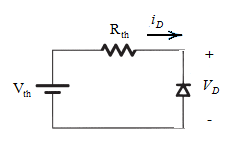
The diode is operating in a reversed biased region as the positive side of the battery is connected to the cathode terminal of diode.
Hence, the ideal diode will behave as an open circuit.
So,
Terminal voltage can be calculated by applying mesh law in the circuit:
By putting the given values and from equation (1):
Case 2:
When anode terminal of the diode is connected to the positive terminal of battery.
The Thevenin equivalent circuit with diode connected as given can be drawn as:
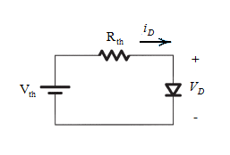
The diode is operating in forward biased region as the positive side of the battery is connected to the anode terminal of diode.
As it is ideal diode, the cut-in voltage across it will be 0.
Hence,
Current can be calculated by applying mesh law in the circuit:
By putting the given values and from equation (2):
Want to see more full solutions like this?
Chapter 4 Solutions
MICROELECTRONIC CIRCUITS(LOOSE)


- An inter-connect bar is used in a device designed to operate between -20℃ and 60℃. It is 0.5mm long with a cross-sectional area of 0.025 mm2 and has to carry a current of 54 µA when a potential difference of 0.5 V is applied to it. B) The bar is made from silicon doped with acceptor atoms. Calculate the concentration of majority carriers and hence that of the acceptor atoms, assuming that the contribution of the minority carriers is negligible. Determine the minority carrier concentration please solve as soon as possiblearrow_forwardQ1) Conduct an evaluation on the practical applications of the concepts of electromagnetism and submit a written report which includes the following. a) Design a circuit which utilizes the concept of electromagnetism and submit a simulation circuit for the same (use simulation tool of your choice) b) Write down the selected values of the components used for example the values of resistors, transistor used, capacitors etc c) Obtain the output for the ciruit using any sinks like CRO, loud speakers etc. d) Discuss about the principles of electromagnetism used in the simulation I WANT QUESTION (D)arrow_forwardA junction employs ND = 5 × 1017 cm−3and NA = 4 × 1016 cm−3.(a) Determine the majority and minoritycarrier concentrations on both sides.(b) Calculate the built-in potential atT = 250 K, 300 K, and 350 K. Explainthe trend.arrow_forward
- For the Zener diode network of Fig. 1 Determine VL, VR, R and PZAssume that the Zener diode is in the “ON" stateWhere: VL = VZ & R = 9375Ωarrow_forwardn-type silicon wafers with a resistivity of 3.0Ω·cm are needed for integrated circuit fabrication. What donor concentration ND is required in the wafers? Assume NA =0.arrow_forwardThe network of Figure below is the basic biasing arrangement for the field-effect transistor (FET), a device of increasing importance in electronic design. (Biasing simply means the application of de levels to establish a particular set of operating conditions.) Even though you may be unfamiliar with the FET, you can perform the following analysis using only the basic laws introduced in your lectures and the information provided on the diagram. a. Determine the voltages VG and Vs. b. Find the currents 11, 12, Ip, and Is. c. Determine Vps. d. Calculate VDG-arrow_forward
- Given the schematic below, assume D1 and D2 are silicon with forward voltages of 0.7V. Find the following (with solutions) a) Conditions required wherein none of the diodes are conducting b) If both diodes are not conduction, what is Vo? Express in terms of Vi c) Plot the overall relationship of Vo and Vi in the coordinate system shown below. Remember, you are to plot the transfer characteristics of the circuit.arrow_forwardConsider a p-n junction at 25 C with a reverse saturation current 10^-9 A. Calculate the voltage drop across the solar cell when it is carrying the 1 A and 10Aarrow_forwardFor the attenuator circuit shown, assume C1 and C2 to be very large (∞) capacitors. Don’t be thrown off by the capacitors (How do they behave at DC? How do they behave at AC if C =∞). Assume D1 and D2 are identical diodes with n=1, V T = 25 mV (use the exponential model). a. Determine the value of the dc voltage, V_N when I = 1mA. b. Draw the small-signal equivalent circuit, replacing the diodes with their small signal resistive model, r_d. c. Determine the value of V_o/V_s when I = 1mA.arrow_forward
- A cathodic protection system is to be designed for a 600 m long and 110 mm diameter buried pipeline coated with fusion bonded epoxy (FBE). The current density required for FBE coated structures is 0.18 mA/m^2. It is required to use horizontal anodes 8 ft. below the ground with 15 ft. spacing. The anode material available is high silicon-cast iron with a consumption rate of 0.5 kg/A-yr. The diameter and length of anodes are 30 cm and 300 cm respeqtively. The weight of each anode is 50 kg. Anode to soil resistance is measured to be 0.24 ohm. The soil resistivity is 2,500 ohm-cm. It is aimed to protect the structure for a period of 22 years. In order to design this CP system, determine, (a) Current required (A) (b) Total number of anodes (c) Total resistance (d) The potential (E) for protection (e) Total power required for this CP system.arrow_forwarda. SketchtheoutputvoanddeterminethedcleveloftheoutputforthenetworkofFig.2.49. Repeat part (a) if the ideal diode is replaced by a silicon diode. Repeat parts (a) and (b) if Vm is increased to 200 V, and compare solutions using Eqs. (2.7) and (2.8).arrow_forwardSurface barrier diodes have a lower noise figure in high frequencies True False The capacitance of the Varactor diode increases with an increase in reverse bias voltage True False The dark current is a current that will exist with no applied illumination True False The lifetime of LCDs is longer than that of LEDs True False The liquid-crystal display (LCD) has the distinct advantage of having a lower power requirement than the LED (light emitting diodes) True Falsearrow_forward
 Delmar's Standard Textbook Of ElectricityElectrical EngineeringISBN:9781337900348Author:Stephen L. HermanPublisher:Cengage Learning