
COMPUTER SCIENCE ILLUMINATED
7th Edition
ISBN: 9781284208047
Author: Dale
Publisher: JONES+BART
expand_more
expand_more
format_list_bulleted
Videos
Question
Chapter 4, Problem 62E
Program Plan Intro
Circuit:
- The circuit is known as the combination of gates that is used to achieve a difficult logical operation.
- It has two general categories, they are:
- Combinational circuit
- Sequential circuit
Expert Solution & Answer
Explanation of Solution
Given circuit:
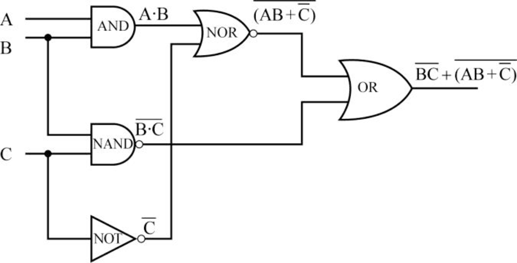
Behavior of the circuit:
- From the above circuit diagram,
- First, the inputs A and B are passed to AND gate to perform the product of A and B and produce the output as
- Next, pass the same input B from the AND gate, and input C is passed in the NAND gate to perform the inverse of product of B and C and produce the output as
- Next, pass the same input C from the NAND gate to NOT gate, to perform the inverse of C to produce the output as
- Next, pass the output of AND gate and output of NOT gate as the input to NOR gate to perform the inverse of sum of “
- Finally, the output of NOR gate and output of NAND gate is passed as the input of OR gate.
- Therefore, “
- Therefore, “
- First, the inputs A and B are passed to AND gate to perform the product of A and B and produce the output as
Truth table for the above circuit diagram:
Step 1:
- The inputs are A, B, and C for the circuit diagram:
| A | B | C | |||||
| 0 | 0 | 0 | |||||
| 0 | 0 | 1 | |||||
| 0 | 1 | 0 | |||||
| 0 | 1 | 1 | |||||
| 1 | 0 | 0 | |||||
| 1 | 0 | 1 | |||||
| 1 | 1 | 0 | |||||
| 1 | 1 | 1 |
Step 2:
- When the inputs are A as 0, B as 0, and C as 0:
| A | B | C | |||||
| 0 | 0 | 0 | 0 | 1 | 1 | 0 | 1 |
| 0 | 0 | 1 | |||||
| 0 | 1 | 0 | |||||
| 0 | 1 | 1 | |||||
| 1 | 0 | 0 | |||||
| 1 | 0 | 1 | |||||
| 1 | 1 | 0 | |||||
| 1 | 1 | 1 |
- First, the inputs A as 0 and B as 0 are passed to AND gate to perform the product of 0 and 0 and produce the output as
- Next, pass the same input B as 0 from the AND gate
- Next, pass the same input C as 0 from the NAND gate
- Next, pass the output of AND gate and output of NOT gate as the input for NOR gate to perform the inverse of sum of “0” and “1”, and produce the output as
- Finally, the output of NOR gate and output of NAND gate is passed as the input of OR gate.
- Therefore, “0” and “1” are passed as input to OR gate and produce the output as
- Therefore, “0” and “1” are passed as input to OR gate and produce the output as
Step 3:
- When the inputs are A as 0, B as 0, and C as 1:
| A | B | C | |||||
| 0 | 0 | 0 | 0 | 1 | 1 | 0 | 1 |
| 0 | 0 | 1 | 0 | 1 | 0 | 1 | 1 |
| 0 | 1 | 0 | |||||
| 0 | 1 | 1 | |||||
| 1 | 0 | 0 | |||||
| 1 | 0 | 1 | |||||
| 1 | 1 | 0 | |||||
| 1 | 1 | 1 |
- First, the inputs A as 0 and B as 0 are passed to AND gate to perform the product of 0 and 0 and produce the output as
- Next, pass the same input B as 0 from the AND gate
- Next, pass the same input C as 1 from the NAND gate
- Next, pass the output of AND gate and output of NOT gate as the input for NOR gate to perform the inverse of sum of “0” and “0” and produces the output as
- Finally, the output of NOR gate and output of NAND gate is passed as the input of OR gate.
- Therefore, “1” and “1” are passed as input to OR gate and produce the output as
- Therefore, “1” and “1” are passed as input to OR gate and produce the output as
Step 4:
- When the inputs are A as 0, B as 1, and C as 0:
| A | B | C | |||||
| 0 | 0 | 0 | 0 | 1 | 1 | 0 | 1 |
| 0 | 0 | 1 | 0 | 1 | 0 | 1 | 1 |
| 0 | 1 | 0 | 0 | 1 | 1 | 0 | 1 |
| 0 | 1 | 1 | |||||
| 1 | 0 | 0 | |||||
| 1 | 0 | 1 | |||||
| 1 | 1 | 0 | |||||
| 1 | 1 | 1 |
- First, the inputs A as 0 and B as 1 are passed to AND gate to perform the product of 0 and 1 and produce the output as
- Next, pass the same input B as 1 from the AND gate
- Next, pass the same input C as 0 from the NAND gate
- Next, pass the output of AND gate and output of NOT gate as the input for NOR gate to perform the inverse of sum of “0” and “1” and produces the output as
- Finally, the output of NOR gate and output of NAND gate are passed as the input of OR gate.
- Therefore, “0” and “1” are passed as input to OR gate and produce the output as
- Therefore, “0” and “1” are passed as input to OR gate and produce the output as
Step 5:
- When the inputs are A as 0, B as 1, and C as 1:
| A | B | C | |||||
| 0 | 0 | 0 | 0 | 1 | 1 | 0 | 1 |
| 0 | 0 | 1 | 0 | 1 | 0 | 1 | 1 |
| 0 | 1 | 0 | 0 | 1 | 1 | 0 | 1 |
| 0 | 1 | 1 | 0 | 0 | 0 | 1 | 1 |
| 1 | 0 | 0 | |||||
| 1 | 0 | 1 | |||||
| 1 | 1 | 0 | |||||
| 1 | 1 | 1 |
- First, the inputs A as 0 and B as 1 are passed to AND gate to perform the product of 0 and 1 and produce the output as
- Next, pass the same input B as 1 from the AND gate
- Next, pass the same input C as 1 from the NAND gate
- Next, pass the output of AND gate and output of NOT gate as the input for NOR gate to perform the inverse of sum of “0” and “0” and produces the output as
- Finally, the output of NOR gate and output of NAND gate are passed as the input of OR gate.
- Therefore, “1” and “0” are passed as input to OR gate and produce the output as
- Therefore, “1” and “0” are passed as input to OR gate and produce the output as
Step 6:
- When the inputs are A as 1, B as 0, and C as 0:
| A | B | C | |||||
| 0 | 0 | 0 | 0 | 1 | 1 | 0 | 1 |
| 0 | 0 | 1 | 0 | 1 | 0 | 1 | 1 |
| 0 | 1 | 0 | 0 | 1 | 1 | 0 | 1 |
| 0 | 1 | 1 | 0 | 0 | 0 | 1 | 1 |
| 1 | 0 | 0 | 0 | 1 | 1 | 0 | 1 |
| 1 | 0 | 1 | |||||
| 1 | 1 | 0 | |||||
| 1 | 1 | 1 |
- First, the inputs A as 1 and B as 0 are passed to AND gate to perform the product of 0 and 1 and produce the output as
- Next, pass the same input B as 0 from the AND gate
- Next, pass the same input C as 0 from the NAND gate
- Next, pass the output of AND gate and output of NOT gate as the input for NOR gate to perform the inverse of sum of “0” and “1” and produces the output as
- Finally, the output of NOR gate and output of NAND gate are passed as the input of OR gate.
- Therefore, “0” and “1” are passed as input to OR gate and produce the output as
- Therefore, “0” and “1” are passed as input to OR gate and produce the output as
Step 7:
- When the inputs are A as 1, B as 0, and C as 1:
| A | B | C | |||||
| 0 | 0 | 0 | 0 | 1 | 1 | 0 | 1 |
| 0 | 0 | 1 | 0 | 1 | 0 | 1 | 1 |
| 0 | 1 | 0 | 0 | 1 | 1 | 0 | 1 |
| 0 | 1 | 1 | 0 | 0 | 0 | 1 | 1 |
| 1 | 0 | 0 | 0 | 1 | 1 | 0 | 1 |
| 1 | 0 | 1 | 0 | 1 | 0 | 1 | 1 |
| 1 | 1 | 0 | |||||
| 1 | 1 | 1 |
- First, the inputs A as 1 and B as 0 are passed to AND gate to perform the product of 0 and 1 and produce the output as
- Next, pass the same input B as 0 from the AND gate
- Next, pass the same input C as 1 from the NAND gate
- Next, pass the output of AND gate and output of NOT gate as the input for NOR gate to perform the inverse of sum of “0” and “0” and produces the output as
- Finally, the output of NOR gate and output of NAND gate are passed as the input of OR gate.
- Therefore, “1” and “1” are passed as input to OR gate and produce the output as
- Therefore, “1” and “1” are passed as input to OR gate and produce the output as
Step 8:
- When the inputs are A as 1, B as 1, and C as 0:
| A | B | C | |||||
| 0 | 0 | 0 | 0 | 1 | 1 | 0 | 1 |
| 0 | 0 | 1 | 0 | 1 | 0 | 1 | 1 |
| 0 | 1 | 0 | 0 | 1 | 1 | 0 | 1 |
| 0 | 1 | 1 | 0 | 0 | 0 | 1 | 1 |
| 1 | 0 | 0 | 0 | 1 | 1 | 0 | 1 |
| 1 | 0 | 1 | 0 | 1 | 0 | 1 | 1 |
| 1 | 1 | 0 | 1 | 1 | 1 | 0 | 1 |
| 1 | 1 | 1 |
- First, the inputs A as 1 and B as 1 are passed to AND gate to perform the product of 1 and 1 and produce the output as
- Next, pass the same input B as 1 from the AND gate
- Next, pass the same input C as 0 from the NAND gate
- Next, pass the output of AND gate and output of NOT gate as the input for NOR gate to perform the inverse of sum of “1” and “1” and produces the output as
- Finally, the output of NOR gate and output of NAND gate are passed as the input of OR gate.
- That is, “0” and “1” are passed as input to OR gate and produce the output as
- That is, “0” and “1” are passed as input to OR gate and produce the output as
Step 9:
- When the inputs are A as 1, B as 1, and C as 1:
| A | B | C | |||||
| 0 | 0 | 0 | 0 | 1 | 1 | 0 | 1 |
| 0 | 0 | 1 | 0 | 1 | 0 | 1 | 1 |
| 0 | 1 | 0 | 0 | 1 | 1 | 0 | 1 |
| 0 | 1 | 1 | 0 | 0 | 0 | 1 | 1 |
| 1 | 0 | 0 | 0 | 1 | 1 | 0 | 1 |
| 1 | 0 | 1 | 0 | 1 | 0 | 1 | 1 |
| 1 | 1 | 0 | 1 | 1 | 1 | 0 | 1 |
| 1 | 1 | 1 | 1 | 0 | 0 | 0 | 0 |
- First, the inputs A as 1 and B as 1 are passed to AND gate to perform the product of 1 and 1 and produce the output as
- Next, pass the same input B as 1 from the AND gate
- Next, pass the same input C as 1 from the NAND gate
- Next, pass the output of AND gate and output of NOT gate as the input for NOR gate to perform the inverse of sum of “1” and “0” and produces the output as
- Finally, the output of NOR gate and output of NAND gate are passed as the input of OR gate.
- Thus, “0” and “0” are passed as input to OR gate and produce the output as
- Thus, “0” and “0” are passed as input to OR gate and produce the output as
Therefore, the truth table for the given circuit is:
| A | B | C | |||||
| 0 | 0 | 0 | 0 | 1 | 1 | 0 | 1 |
| 0 | 0 | 1 | 0 | 1 | 0 | 1 | 1 |
| 0 | 1 | 0 | 0 | 1 | 1 | 0 | 1 |
| 0 | 1 | 1 | 0 | 0 | 0 | 1 | 1 |
| 1 | 0 | 0 | 0 | 1 | 1 | 0 | 1 |
| 1 | 0 | 1 | 0 | 1 | 0 | 1 | 1 |
| 1 | 1 | 0 | 1 | 1 | 1 | 0 | 1 |
| 1 | 1 | 1 | 1 | 0 | 0 | 0 | 0 |
Want to see more full solutions like this?
Subscribe now to access step-by-step solutions to millions of textbook problems written by subject matter experts!
Chapter 4 Solutions
COMPUTER SCIENCE ILLUMINATED
Ch. 4 - Prob. 1ECh. 4 - Prob. 2ECh. 4 - Prob. 3ECh. 4 - Prob. 4ECh. 4 - Prob. 5ECh. 4 - Prob. 6ECh. 4 - Prob. 7ECh. 4 - Prob. 8ECh. 4 - Prob. 9ECh. 4 - Prob. 10E
Ch. 4 - Prob. 11ECh. 4 - Prob. 12ECh. 4 - Prob. 13ECh. 4 - Prob. 14ECh. 4 - Prob. 15ECh. 4 - Prob. 16ECh. 4 - Prob. 17ECh. 4 - Prob. 18ECh. 4 - Prob. 19ECh. 4 - Prob. 20ECh. 4 - Prob. 21ECh. 4 - Prob. 22ECh. 4 - Prob. 23ECh. 4 - Prob. 24ECh. 4 - Prob. 25ECh. 4 - Prob. 26ECh. 4 - Prob. 27ECh. 4 - Prob. 28ECh. 4 - Prob. 29ECh. 4 - Prob. 30ECh. 4 - Prob. 31ECh. 4 - Prob. 32ECh. 4 - Prob. 33ECh. 4 - Prob. 34ECh. 4 - Prob. 35ECh. 4 - Prob. 36ECh. 4 - Prob. 37ECh. 4 - Prob. 38ECh. 4 - Prob. 39ECh. 4 - Prob. 40ECh. 4 - Prob. 41ECh. 4 - Prob. 42ECh. 4 - Prob. 43ECh. 4 - Prob. 44ECh. 4 - Prob. 45ECh. 4 - Prob. 46ECh. 4 - Prob. 47ECh. 4 - Prob. 48ECh. 4 - Prob. 49ECh. 4 - Prob. 50ECh. 4 - Prob. 51ECh. 4 - Prob. 52ECh. 4 - Prob. 53ECh. 4 - Prob. 54ECh. 4 - Prob. 55ECh. 4 - Prob. 56ECh. 4 - Prob. 57ECh. 4 - Prob. 58ECh. 4 - Prob. 59ECh. 4 - Prob. 60ECh. 4 - Prob. 61ECh. 4 - Prob. 62ECh. 4 - Prob. 63ECh. 4 - Prob. 64ECh. 4 - Prob. 65ECh. 4 - Prob. 66ECh. 4 - Prob. 67ECh. 4 - Prob. 68ECh. 4 - Prob. 69ECh. 4 - Prob. 70ECh. 4 - Prob. 71ECh. 4 - Prob. 72ECh. 4 - Prob. 73ECh. 4 - Prob. 1TQCh. 4 - Prob. 2TQCh. 4 - Prob. 3TQCh. 4 - Prob. 4TQ
Knowledge Booster


Learn more about
Need a deep-dive on the concept behind this application? Look no further. Learn more about this topic, computer-science and related others by exploring similar questions and additional content below.Recommended textbooks for you
 Database System ConceptsComputer ScienceISBN:9780078022159Author:Abraham Silberschatz Professor, Henry F. Korth, S. SudarshanPublisher:McGraw-Hill Education
 Starting Out with Python (4th Edition)Computer ScienceISBN:9780134444321Author:Tony GaddisPublisher:PEARSON
 Digital Fundamentals (11th Edition)Computer ScienceISBN:9780132737968Author:Thomas L. FloydPublisher:PEARSON
 C How to Program (8th Edition)Computer ScienceISBN:9780133976892Author:Paul J. Deitel, Harvey DeitelPublisher:PEARSON
 Database Systems: Design, Implementation, & Manag...Computer ScienceISBN:9781337627900Author:Carlos Coronel, Steven MorrisPublisher:Cengage Learning
 Programmable Logic ControllersComputer ScienceISBN:9780073373843Author:Frank D. PetruzellaPublisher:McGraw-Hill Education
Database System Concepts
Computer Science
ISBN:9780078022159
Author:Abraham Silberschatz Professor, Henry F. Korth, S. Sudarshan
Publisher:McGraw-Hill Education
Starting Out with Python (4th Edition)
Computer Science
ISBN:9780134444321
Author:Tony Gaddis
Publisher:PEARSON
Digital Fundamentals (11th Edition)
Computer Science
ISBN:9780132737968
Author:Thomas L. Floyd
Publisher:PEARSON
C How to Program (8th Edition)
Computer Science
ISBN:9780133976892
Author:Paul J. Deitel, Harvey Deitel
Publisher:PEARSON
Database Systems: Design, Implementation, & Manag...
Computer Science
ISBN:9781337627900
Author:Carlos Coronel, Steven Morris
Publisher:Cengage Learning
Programmable Logic Controllers
Computer Science
ISBN:9780073373843
Author:Frank D. Petruzella
Publisher:McGraw-Hill Education
Boolean Algebra - Digital Logic and Logic Families - Industrial Electronics; Author: Ekeeda;https://www.youtube.com/watch?v=u7XnJos-_Hs;License: Standard YouTube License, CC-BY
Boolean Algebra 1 – The Laws of Boolean Algebra; Author: Computer Science;https://www.youtube.com/watch?v=EPJf4owqwdA;License: Standard Youtube License