
Concept explainers
Videos
For the transistor configuration in Fig. 8.126:
a. Solve for the currents
b. Find the voltages
c. What is the ratio of output current
[Note: In transistor analysis, this ratio is referred to as the dc beta of the transistor (
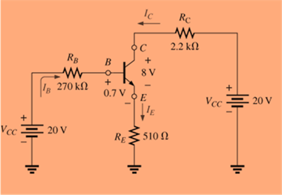
Fig. 8.126
Want to see the full answer?
Check out a sample textbook solution
Chapter 8 Solutions
Laboratory Manual for Introductory Circuit Analysis


- (7) Determine IB, IC, IE, VB,and Vc in the following figure, where BDC is 48. IF www Re 12KQ Rc 1.2KQ Vac 201 FIFarrow_forwardQ1) find for given circuit below. 1.a. What circuit is shown on the image above and what is gain ? 1.b. If R2 is 40x higher than R1 what will happen to node 2? Provide waveform and explain why it happens. 1.c. Modify the circuit to have an overall gain of 2. Provide photosarrow_forward8. For the circuit shown in Fig.8, draw the d.c. load line. Ic Rc= 5 k2 NO SIGNAL 15 V Fig 8arrow_forward
- A) For the drauit of Figure 8, determine the following parameters: Ig, Ip, Vas, VD. VBc and then state the mode in which the BJT is operating. Useeither the gaphical (using a graph paper) approach or the mathematical approach Vcc Given: RC Vcc = 20 V R3 IDss = 8 mA %3D Vc p =-4 V Vss =-1V B =100 Vo RB = 470 2 %3! Rc = 36 k2 Rs =1 k2 RG RG = 2 MN Rs Vssarrow_forwardGiven that VBE = 0.7 V and using the values from the table: VCC (V) 10 BETA 156 Calculate the following: Part A.(DC Analysis) 1. IB 2. Ic 3. VCE R1 12kohms R2 4kohms RC 1075ohms RE 450ohmsarrow_forward1.a. What circuit is shown on the image above? 1.b. What is the gain? 1.c. If R2 is 40x higher than R1 what will happen to node 2? Provide waveform and explain why it happens. 1.d. Modify the circuit to have an overall gain of 2. Provide photos.arrow_forward
- 3. The network of Figure below is the basic biasing arrangement for the field-effect transistor (FET), a device of increasing importance in electronic design. (Biasing simply means the application of de levels to establish a particular set of operating conditions.) Even though you may be unfamiliar with the FET, you can perform the following analysis using only the basic laws introduced in your lectures and the information provided on the diagram. a. Determine the voltages VG and Vs. b. Find the currents I1, I2, ID, and Is. c. Determine VDS- d. Calculate DG- VDD = 16 V to ID 2 MN Rp32.5 kN R1 오D VGO VGs = -1.75 V IG = 0 A Ip = Is I IG VGS Is OVs R2 270 k2 Rs 1.5 kNarrow_forward3. The network of Figure below is the basic biasing arrangement for the field-effect transistor (FET), a device of increasing importance in electronic design. (Biasing simply means the application of de levels to establish a particular set of operating conditions.) Even though you may be unfamiliar with the FET, you can perform the following analysis using only the basic laws introduced in your lectures and the information provided on the diagram. a. Determine the voltages VG and Vs. b. Find the currents I1, 12, Ip, and Is. c. Determine VDs. d. Calculate VDG. VDD = 16 V ID 2 MN Rp 2.5 kn R1 오D VGO G = -1.75 V 2l V s O's Is Ic = 0 A Ip = Is R2 270 kn Rs 1.5 kNarrow_forward3. The network of Figure below is the basic biasing arrangement for the field-effect transistor (FET), a device of increasing importance in electronic design. (Biasing simply means the application of de levels to establish a particular set of operating conditions.) Even though you may be unfamiliar with the FET, you can perform the following analysis using only the basic laws introduced in your lectures and the information provided on the diagram. a. Determine the voltages VG and Vs. b. Find the currents h, h, In, and Is. c. Determine Vns. d. Calculate VDG. VDD - 16 V 오 2 Mn Ro25 kn OD Vas - -1.75 V 4 T I6 - 0A In = Is Ves o's R270 knarrow_forward
- 3. The network of Figure below is the basic biasing arrangement for the field-effect transistor (FET), a device of increasing importance in electronic design. (Biasing simply means the application of de levels to establish a particular set of operating conditions.) Even though you may be unfamiliar with the FET, you can perform the following analysis using only the basic laws introduced in your lectures and the information provided on the diagram. a. Determine the voltages VG and Vs. b. Find the currents I1, I2, ID, and Is. c. Determine Vps. d. Calculate V DG- VDD = 16 V to \ID 32 MN Rp32.5 kN R1 OD VGO Vas = -1.75 V h| IG S VGS IG O's Is = 0 A Ip = Is R2 270 kN %3D Rs 1.5 kNarrow_forward3. The network of Figure below is the basic biasing arrangement for the field-effect transistor (FET), a device of increasing importance in electronic design. (Biasing simply means the application of de levels to establish a particular set of operating conditions.) Even though you may be unfamiliar with the FET, you can perform the following analysis using only the basic laws introduced in your lectures and the information provided on the diagram. a. Determine the voltages Vg and V's. b. Find the currents I1, I2, Ip, and Is. c. Determine Vos. d. Calculate VpG. Vpo = 16 V 오 R1 2 Mn Rp2.5 kn OD VGO Ves = -1.75 V IG - 0A In - Is VGS o's Is IS R2 270 kf Rs 1.5 knarrow_forward3. The network of Figure below is the basic biasing arrangement for the field-effect transistor (FET), a device of increasing importance in electronic design. (Biasing simply means the application of de levels to establish a particular set of operating conditions.) Even though you may be unfamiliar with the FET, you can perform the following analysis using only the basic laws introduced in your lectures and the information provided on the diagram. a. Determine the voltages VG and Vs. b. Find the currents I1, I2, ID, and Is. c. Determine V Ds- d. Calculate VpG- VDD = 16 V 오 ID R1 2 ΜΩ Rp 2.5 kN OD VGO IG VGs = -1.75 V 2 VGS IG = 0 A In = Is o's |Is R2 270 kN Rs 1.5 kNarrow_forward
 Introductory Circuit Analysis (13th Edition)Electrical EngineeringISBN:9780133923605Author:Robert L. BoylestadPublisher:PEARSON
 Delmar's Standard Textbook Of ElectricityElectrical EngineeringISBN:9781337900348Author:Stephen L. HermanPublisher:Cengage Learning
 Programmable Logic ControllersElectrical EngineeringISBN:9780073373843Author:Frank D. PetruzellaPublisher:McGraw-Hill Education
 Fundamentals of Electric CircuitsElectrical EngineeringISBN:9780078028229Author:Charles K Alexander, Matthew SadikuPublisher:McGraw-Hill Education
 Electric Circuits. (11th Edition)Electrical EngineeringISBN:9780134746968Author:James W. Nilsson, Susan RiedelPublisher:PEARSON
 Engineering ElectromagneticsElectrical EngineeringISBN:9780078028151Author:Hayt, William H. (william Hart), Jr, BUCK, John A.Publisher:Mcgraw-hill Education,