
Concept explainers
Videos
Design an ideal inverting op-amp circuit such that the voltage gain is
(a)
The value of the resistance
Answer to Problem 9.1EP
Thevalue of the resistance
Explanation of Solution
Calculation:
The given diagram is shown in Figure 1
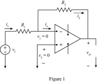
The above op-amp is considered to be ideal.
The value of the voltage
The expression for the input voltage is given by,
Substitute
Apply KCL at negative terminal.
Substitute
The expression for the value of the voltage gain is given by,
The expression for the value of the current
Substitute
Substitute
Substitute
Substitute
Substitute
Substitute
The expression for the maximum value of the current is given by,
The expression for the maximum current is given by,
Substitute
The expression for the minimum value of the resistance
Substitute
The expression for the minimum value of the resistance
Substitute
Conclusion:
Therefore, the value of the resistance
(b)
The value for the range of the output voltage
Answer to Problem 9.1EP
The range of the output voltage is
Explanation of Solution
Calculation:
The expression for the variation of the output voltage is given by,
From above the variation of the voltage is given by,
Conclusion:
Therefore, the range of the output voltage is
Want to see more full solutions like this?
Chapter 9 Solutions
Microelectronics Circuit Analysis and Design
Additional Engineering Textbook Solutions
Electrical Engineering: Principles & Applications (7th Edition)
Programmable Logic Controllers
ANALYSIS+DESIGN OF LINEAR CIRCUITS(LL)
Basic Engineering Circuit Analysis
Principles and Applications of Electrical Engineering
ELECTRICITY FOR TRADES (LOOSELEAF)


- If they are defined as R1=12Ω, R2=5Ω and VS=5V respectively in the circuit given below, how many amps is the İ1 ambient current value? Help me please... Thank you so much.arrow_forwardRefer to the circuit shown, where the op amp is assumed to be ideal. Given that Ra=3 kΩ, Rb=5 kΩ, Rc=25 kΩ, va=150 mV, vb=100 mV, vc=250 mV, and VCC=±6 V, specify the range of Rf for which the op amp operates within its linear region.arrow_forwardIs it possible to get a gain less than unity using a non-inverting amplifier configuration? If yes, sketch a circuit.''please solve it in computer font, not on paper''arrow_forward
- Assume that the op amp in the circuit shown is ideal. 1. Calculate vo for the following values of vs: 0.4, 2.0, 3.5, −0.6, −1.6, and −2.4 V. 2. Specify the range of vs required to avoid amplifier saturation.arrow_forwardThe op amp in the circuit shown is ideal: RI= 3KΩ, RF1=2KΩ, RF2=6KΩ, RL=10KΩ, RA=RB= 1KΩ, Vin=10V 1.1) Calculate Vout 1.2) Calculate Iaarrow_forwardThe inverting amplifier in the circuit shown has an input resistance of 500 kΩ, an output resistance of 5 kΩ, and an open-loop gain of 300,000. Assume that the amplifier is operating in its linear region. 1. Calculate the voltage gain (vo/vg) of the amplifier. 2. Calculate the value of vn in microvolts when vg=1 V. 3. Calculate the resistance seen by the signal source (vg). 4. Repeat (a)–(c) using the ideal model for the op amp.arrow_forward
- An operational amplifier has a high input impedance and low output impedance. Do you think having those impedance are good or not? Explain your answer.arrow_forwardFor the circuit above, R= 4MΩ and C = 0.75μF. Vi(t)= −t^2V for 0s≤t≤5s. What is the value of Vo at time t=5s, if Vo(0) = 0? You can assume the operational amplifier behaves as an ideal op amp with power supplies of +15 and -15. Give your answer in volts.arrow_forwardDesign a combinational circuit with three inputs (E,L,Y) and three outputs (F,R,A). If the input is less than 5, then the output is 2 greater than the input. Otherwise, the output is 3 less than the input. if E=0 L=0 and Y=0, then if E=0 L=0 and Y=1, then if E=0 L=1 and Y=0, then if E=0 L=1 and Y=1, then…arrow_forward
- The op amp in the circuit shown is ideal. 1. Calculate vo if va=1 V and vb=0 V. 2. Repeat (a) for va=1 V and vb=2 V. 3. If va=1.5 V, specify the range of vb that avoids amplifier saturation.arrow_forwardThe op amp in the circuit of Figure is ideal. What op amp circuit configuration isthis? Calculate ?0.arrow_forwardThe op amp as shown is used to increase the overall output resistance of current source M1. If VREF = 5V, VDD = 0 V, VSS = 15 V, R = 50 kΩ, Kn = 800 μA/V2, VT N = 0.8 V, λ = 0.02 V−1, and A = 50,000, what are the output current Io and output resistance of the current source?arrow_forward
 Introductory Circuit Analysis (13th Edition)Electrical EngineeringISBN:9780133923605Author:Robert L. BoylestadPublisher:PEARSON
 Delmar's Standard Textbook Of ElectricityElectrical EngineeringISBN:9781337900348Author:Stephen L. HermanPublisher:Cengage Learning
 Programmable Logic ControllersElectrical EngineeringISBN:9780073373843Author:Frank D. PetruzellaPublisher:McGraw-Hill Education
 Fundamentals of Electric CircuitsElectrical EngineeringISBN:9780078028229Author:Charles K Alexander, Matthew SadikuPublisher:McGraw-Hill Education
 Electric Circuits. (11th Edition)Electrical EngineeringISBN:9780134746968Author:James W. Nilsson, Susan RiedelPublisher:PEARSON
 Engineering ElectromagneticsElectrical EngineeringISBN:9780078028151Author:Hayt, William H. (william Hart), Jr, BUCK, John A.Publisher:Mcgraw-hill Education,