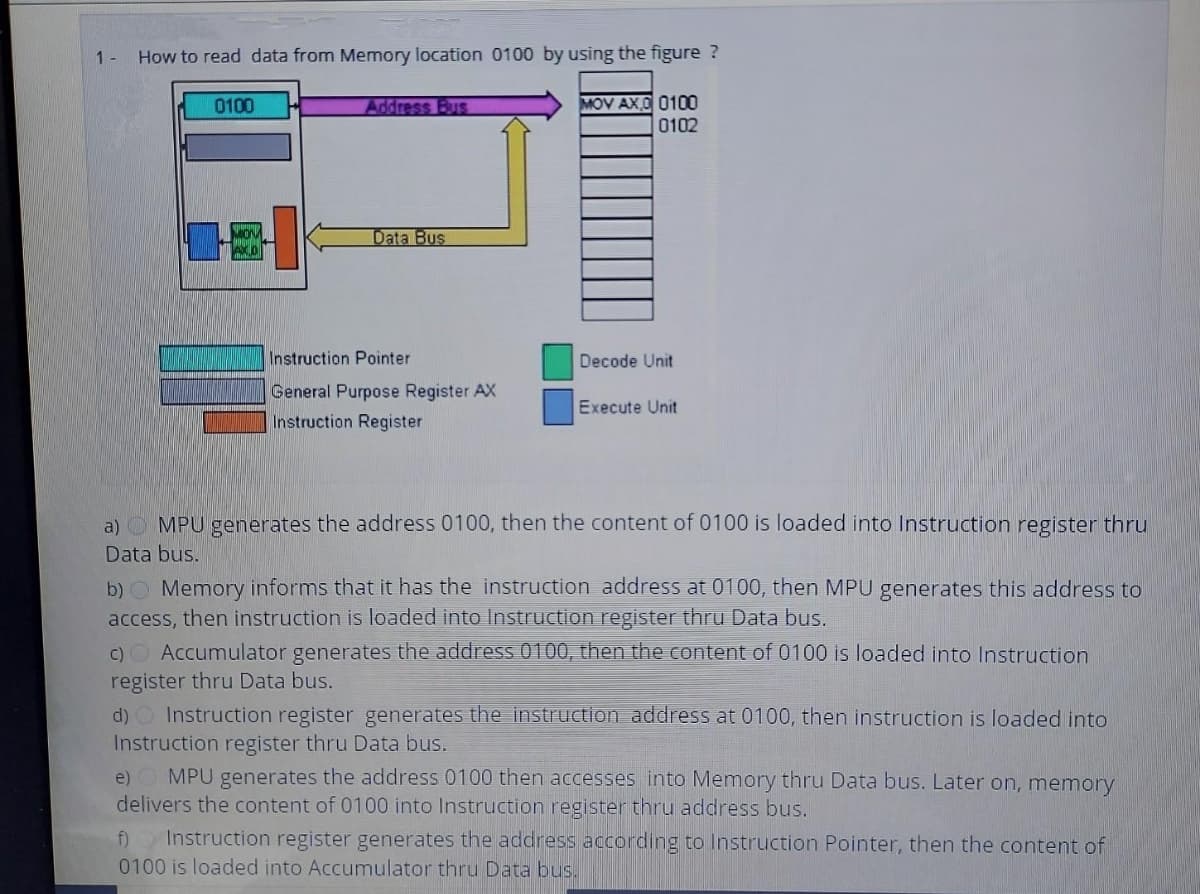
1- How to read data from Memory location 0100 by using the figure ? MOV AX,0 0100 0102 0100 Address Bus Data Bus Instruction Pointer Decode Unit General Purpose Register AX Execute Unit Instruction Register
Q: Q4./DS 2000, SS 3000, BX-012A, BP-021B, DI 0010 SI 0020. 1. Compute the offset of each of the…
A: We solve the question in figure: Figure 1:
Q: A- The Hardware Architecture Shown in Figure (2), is it a Von-Neumann Architecture or Harvard…
A: According to the information given:- We have to find out the mentioned hardware architecture is…
Q: For a 512k x 32 memory system, how wide does the incoming address bus needed to be in order to…
A: Given, Size of memory system = 512k x 32 For a p x q memory system, Size of address bus = log 2 p…
Q: 12. What is the content value for instruction address 803? * PC 804 AC 804 АС 1CC6 PC D4CA IR 5913…
A: Program counter PC stores the address of next instruction. Given address of current instruction is…
Q: What is the correct address range for a microprocessor with 42 address lines? a. 0000000000 -…
A: Actually, binary numbers are nothing but a 0's and 1's.
Q: The Hack architecture partitions the address space and does not allow both data and instructions to…
A: The Hack computer is a 16-bit von Neumann machine, it consists of CPU, separate memory modules for…
Q: 2) A digital computer has a memory unit with 32 pits per word. The instruction set consists of 102…
A: Given:-
Q: 1. A central processing unit (CPU) has the following hardware components: Program Counter (PC) •…
A: All registered CPU - connected to two internal buses Memory Bus
Q: Desired to have a memory of = 64K bytes. No of bits in address bus to address memory location = 13…
A: Desired to have a memory of = 64K bytes.No of bits in address bus to address memory location = 13…
Q: Instructions that when executed provide desired features, functions and performance is a. software…
A: Instructions are the statements that forces hardware to do activities in computer system.
Q: 12. What is the content value for instruction address 803? * PC 804 AC 804 АС 1CC6 PC D4CA IR 5913…
A: Given address of current instruction is 803 The program counter (PC) holds the address of the next…
Q: Table Q15 shows the micro-operations of fetch cycle, interrupt cycle, and execute cycle of the ADD…
A: Here we write micro-operation in simple way:…
Q: 04. Intel 8086 microprocessor: aCan have 16 Mbyte memory. b Canaddress 16address bus lines. S- Can…
A: The Intel 8086 Microprocessor is an updated variant of the Intel 8085 Microprocessor, which was…
Q: Q5: Compare the following [o Stack Segment and Extra Segment Register Control Flag Register and…
A: Answer :- 1) Stack segment and Extra segment register The stack segment register (SS) is usually…
Q: 58. The memory location’s address where data is to be stored is specified by ___________. a. Memory…
A: The Memory Address Register includes the address of the memory location that is to be read from or…
Q: Register Indirect Addressing C.f. indirect addressing EA = (R) %3D Operand is in memory cell pointed…
A: The address of the operand is directly placed in one of the registers in case of Register Indirect…
Q: Stack Segment and Extra Segment Register Control Flag Register and Conditional Flag Register Logical…
A: 1- Extra Segment Register (ES): also refers to a segment in the memory which is another data segment…
Q: Help please mcq After execution the far jump instruction: JMP A3000127h; the new value of Physical…
A: Solution
Q: What are the duties of segment registers? Select one: a. Physical Address b. Offset Address c.…
A: Answer to the given question A segment register changes the memory address accessed by 16 bits at a…
Q: What is the address space of a processor with 32-bit data bus & 32-bit address bus
A: Some of this is based on how your define "32-bit". As a hardware engineer, I think of 32-bit as a…
Q: A 10-bit address bus support(a) 1,000,000 memory addresses (b) 1024 memory addresses(c) 100 memory…
A: Answer: (b) 1024 memory addresses
Q: 3. Explain in paragraph format what is happening in this example: Address >Add Instruction memory…
A: Introduction to Pipelining Pipelining is a method of breaking down a sequential process into…
Q: Q3. Mark True or False, correct when false: a) Address bus is bidirectional b) Data bus is…
A: NOTE: As per our guidelines we are supposed to answer only one question. Kindly repost other…
Q: Suppose that a 64MB system memory is built from 64 1MB RAM chips. How many address lines are needed…
A: Answer :
Q: Q6. Answer True or False for the followings: a) Machine code is the assembly code b) Data field is…
A: machine code is the assembly code data field is 16 bit while address field is 8 bit Trainer kit can…
Q: The Kiwi™ memory architecture design team has a dilemma. The team is considering several different…
A: a) Design 1 logical address width = 12 bits logical memory size = (2^12)bytes page size = 16 bytes…
Q: Instructions Space MAR ALU MBR AC BUS PC Control Data Space Cache A simple processor shown in the…
A: subtraction, addition and multiplication operations are given below:- by bartleby guidelines i am…
Q: 3. A microprocessor has .... ... Data Bus a. unidirectional b. bi-directional с. Both 4. A…
A: Answer : Bi-directional A microprocessor has bi-directional data bus. Explanation: A data bus in a…
Q: A Large Memory with the following buses: Address bus 32 bit. Data bus 32 bit. If we want to build…
A:
Q: Q1: Explain why 8086 Microprocessor have Data line 16 bit and Address line 20 bit.
A: 8086 Microprocessor have data line and address: It is enhanced version it was designed Intel in…
Q: CPU Main Memory Instructions Space MAR ALU MBR АС BUS PC Control Data Space Cache Explain in your…
A: Here it is the architecture of the simple processor, it having the two main blocks those are CPU and…
Q: The PIC 12F508/509 block diagram Program memory Data bus for program memory, carrying instruction…
A: Functions of peripherals (PIC12F508/509):• 6 I/O pins:- 5 I/O pins with individual direction…
Q: CPU Main Memory Instructions Space MAR ALU MBR AC BUS PC Control Data Space Cache Step by step…
A: Given is in a reaction between Fe+3 and NCS-, Kc = 620.4 Volume of Fe+3 = 10 mL molarity of Fe+3 =…
Q: Assume that an Intel CPU has address bus 25-bits wide. What is the maximum addressable memory?…
A: Given: Intel CPU has address bus 25-bits wide .what is maximum addressable memory
Q: 21 - In the microprocessor, the leftmost 3 bits of the 14-bit address bus are reserved for Chip…
A: Given: leftmost 3 bits of the 14-bit address address bus contains 2FBAH find the selected device ID
Q: Take a look at the picture of MIPS 800 Instruction Decode Register Fetch ID Execute Address Calc.…
A:
Q: 1) given the size of the word accessible main memory is 1KB and the size of the word is 16-byte, the…
A: Given Data : Memory size = 1KB Size of memory word = 16 Byte Number of registers = 64
Q: Symmetric multiprocessing architecture of the computer system uses shared a. bus b. memory c.…
A: Let's see all the options: Option (a) : bus Bus is used for transferring data from main memory to…
Q: provide a short explanation on how memory addressing works and why it's important?
A: Addressing Memory: A memory address is a unique address that the device or CPU uses to track…
Q: Explain why 8086 Microprocessor have Data line 16 bit and Address line 20 bit.
A: 8086 microprocessor :- 8086 microprocessor is the enhanced and advanced version of 8085…
Q: processor with 40-bit address pins and 64-bits data pins
A: Given address pins = 40 bits Data pins = 64 bits
Q: Calculate the physical address. Assume DS = 1234h, AX = 4523h with the help of memory diagram. MOV…
A: S. No. 8086 microprocessor 8088 microprocessor 1 The data bus is of 16 bits. The data bus is of…
Q: CPU Main Memory Instructions Space MAR ALU MBR AC BUS PC Control Data Space Cache A simple processor…
A: Given is in a reaction between Fe+3 and NCS-, Kc = 620.4 Volume of Fe+3 = 10 mL molarity of Fe+3 =…
Q: CPU Main Memory Instructions Space MAR ALU MBR AC BUS PC Control Data Space Cache A simple processor…
A: According to the guidelines i can answer only first 3 subparts
Q: Suppose that a 32MB system memory is built from 32 1MB RAM chips. How many address lines are needed…
A: As it is given that there are 32 RAM memory chips. To represent 32 different binary numbers we…
Q: In a computer instruction format, the instruction length is 11 bits and the size of an address field…
A: Given:Instruction length = 11 bits = 211 = 2048 bitsAddress register size = 4 bits
Q: Q6) What is a Volatile and Non-Volatile memory? Show the construction of ROM for 32 x 8 ROM. Q7)…
A: Hi, since there are multiple questions in this post, as per our policy, I'll answer the first…
Q: Question#l: Choose the correct answer 1. In 8086 microprocessor , the address bus is А. 12 bit bit…
A: Correct option is 'd' that is 20 bit wide.
Q: The memory unit of a computer has 2M words of 32 bits each. The computer has an instruction format…
A:
Q: Q5. Given the content of memory and the registers below. i. Indicate the type of addressing mode of…
A: The answer has been given in the below steps:
Step by step
Solved in 2 steps
- 6. Assume that two numbers: dividend and divisor are saved in memory address M1 and M2 respectively. Quotient and remainder should be saved in R1 and R2 respectively. Write assembly language instructions and then list microoperations for each instruction and list the control signals required to be activated for each microoperation. MBR is used as buffer for any register to register transfer operation. Signal Description: Control signals operation Comments C0 MAR to RAM (through address bus) C1 PC to MBR C2 PC to MAR C3 MBR to PC C4 MBR to IR C5 RAM to MBR C6 MBR to ALU C7 Accumulator to ALU C8 IR to MAR C9 ALU to Accumulator C10 MBR to Accumulator C11 Accumulator to MBR C12 MBR to RAM (through data bus) C13 IR to Control Unit C14 MBR to R1 C15 MBR to R2 C16 MBR to R3 C17 MBR to R4…1. The hypothetical machine has two I/O instructions: 0011 = Load AC from I/O 0111 = Store AC to I/O In these cases, the 12-bit address identifies a particular I/O device. List the steps for every execution for the following program and illustrate using table that explain the process below : a. Load AC from device 5. b. Add contents of memory location 940. c. Store AC to device 6. d. Assume that the next value retrieved from device 5 is 3 and that location 940 contains a value of 2. Please pointing a, b,c ans. Because one I already upload this question and I didn't understand which one is and of a...please write ans a, b , c pleaseSuppose a computer using direct mapped cache has 4M byte of byte-addressable main memory, and a cache of 512 blocks, where each cache block contains 64 bytes. a) How many blocks of main memory are there? b) What is the format of a memory address as seen by the cache, i.e., what are the sizes of the tag, block, and offset fields? c) To which cache block will the memory address 0x00007266 map?
- 1. Name all of the general purpose registers and some of their special functions. 2. How are the segment registers used to form a 20-bit address? 3. (a) If CS contains 03E0H and IP contains 1F20H, from what address is the next instruction fetched? (b) If SS contains 0400H and SP contains 3FFEH, where is the top of the stack located? (c) If a data segment deigns at address 24000H, what is the address of the last location in the segment? 4. Explain what the instruction array and data caches are used for. 5. What is the EU and BIU, and what purpose in the microcomputer? 6. Two memory locations, beginning at address 3000H, contain the bytes 34H and 12H. What is the word stored at location 3000H? See Figure 2.26 for details. Address 3000 Data 34 3001 12 Figure 2.26 For question 6 7. What is a physical address? What are the differences between the 8086 logical and physical memory maps? 8. May memory segments overlap? If so, what is the minimum number of overlapped bytes…QUESTION ONE (1) 1. The hypothetical machine has two I/O instructions: 0011 = Load AC from I/O 0111 = Store AC to I/O In these cases, the 12-bit address identifies a particular I/O device. List the steps for every execution for the following program and illustrate using table that explain the process below : a. Load AC from device 5. b. Add contents of memory location 940. c. Store AC to device 6. d. Assume that the next value retrieved from device 5 is 3 and that location 940 contains a value of 2.17. Consider the following hypothetical instruction: SubMem R1, mem1, mem2 This instruction works as follows: \[ \mathrm{R} 1 \leftarrow \text { [mem1] - [mem2] } \] In a multi-cycle datapath implementation, this instruction will: a. Use the MDR twice b. Use the ALU once c. Use the "shift to left" unit twice d. None of the above Answer: B 18. Consider the following hypothetical instruction: Mems mem1, R1, mem2 This instruction works as follows: \[ \text { [mem1] } \leftarrow \mathrm{R} 1 \text { - [mem2] } \] One of the following is correct about this instruction: a. It will not need theBregister b. It will require priting into MDR twice c. It will require writing into the ALUout three times d. None of the above Answer: A 19. By comparing the hypothetical instructions given in Questions (17) and (18), if we run these instructions on the same processor, then one of the following is correct: a. Both instructions have the same CPI b. Mems executes faster than SubMem c. SubMem executes…
- . Consider a system that has multiple processors where eachprocessor has its own cache, but main memory is shared among allprocessors.1. a) Which cache write policy would you use?2. b) The cache coherency problem. With regard to the systemjust described, what problems are caused if a processor has acopy of memory block A in its cache and a second processor,also having a copy of A in its cache, then updates mainmemory block A? Can you think of a way (perhaps morethan one) of preventing this situation, or lessening itseffects?Consider the following instruction:Instruction: Add Rd, Rs, RtInterperation: Reg[Rd] = Reg[Rs] + Reg[Rt] RegWrite MemRead ALUMux MemWrite ALUOp RegMux Branch a, What are the values of control signals generated by the control in Figure 4.2 for the above instruction? b, Which resources (blocks) perform a useful function for this instruction? c, Which resources (blocks) produce outputs, but their outputs are not used for this instruction? d, which resources (blocks) produce no output for this instruction?B) Amain memory address is viewed as consisting of multiple fields. List and define these fields for Direct Mapped Cache, Associative Mapped Cache and Set-associative Mapped Cache Memory.
- Suppose a computer using direct-mapped cache has 232 (that's 232)232) bytes of byte-addressable main memory, and a cache size of 512 bytes, and each cache block contains 64 bytes. How many blocks of main memory are there? What is the format of a memory address as seen by cache, i.e. what are the sizes of the tag, block, and offset fields? To which cache block will the memory address 0x13A4498A map?Assume the following values are stored at the indicated memory addresses and registers Address Value 0x100 0xaaa 0x104 0x123 0x108 0x12 0x10c 0x10 Register Value %eax 0x100 %ecx 0x1 %edx 0x3 Fill up the following table: %eax 0x104 $0x108 (%eax) 4(%eax) 9(%eax,%edx) 260(%ecx,%edx) 0xFC(,%ecx,4) (%eax,%edx,4)Suppose that 16M × 16 memory built using 512K × 8 RAM chips and that memory is word addressable.1. a) How many RAM chips are necessary?2. b) If we were accessing one full word, how many chips would be involved? 3. c) How many address bits are needed for each RAM chip?4. d) How many banks will this memory have?5. e) How many address bits are needed for all memory?6. f) If high-order interleaving is used, where would address 14 (which is E in hex) be located?7. g) Repeat exercise 9f for low-order interleaving.