In the logic circuit shown below, what is the minimum RL that the inverter can drive without causing the output to drop below 4V when Vi = oV? Vcc=+5V 1000 Ra RL 10ka
In the logic circuit shown below, what is the minimum RL that the inverter can drive without causing the output to drop below 4V when Vi = oV? Vcc=+5V 1000 Ra RL 10ka

Chapter22: Sequence Control
Section: Chapter Questions
Problem 6SQ: Draw a symbol for a solid-state logic element AND.

Related questions
Question
i need the answer quickly
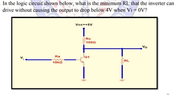
Transcribed Image Text:In the logic circuit shown below, what is the minimum RL that the inverter can
drive without causing the output to drop below 4V when Vi = 0V?
Vcc=+5V
Rc
1000
Vo
Ra
RL
10ka
Expert Solution
This question has been solved!
Explore an expertly crafted, step-by-step solution for a thorough understanding of key concepts.

Step by step
Solved in 2 steps

Knowledge Booster


Learn more about
Need a deep-dive on the concept behind this application? Look no further. Learn more about this topic, electrical-engineering and related others by exploring similar questions and additional content below.Recommended textbooks for you