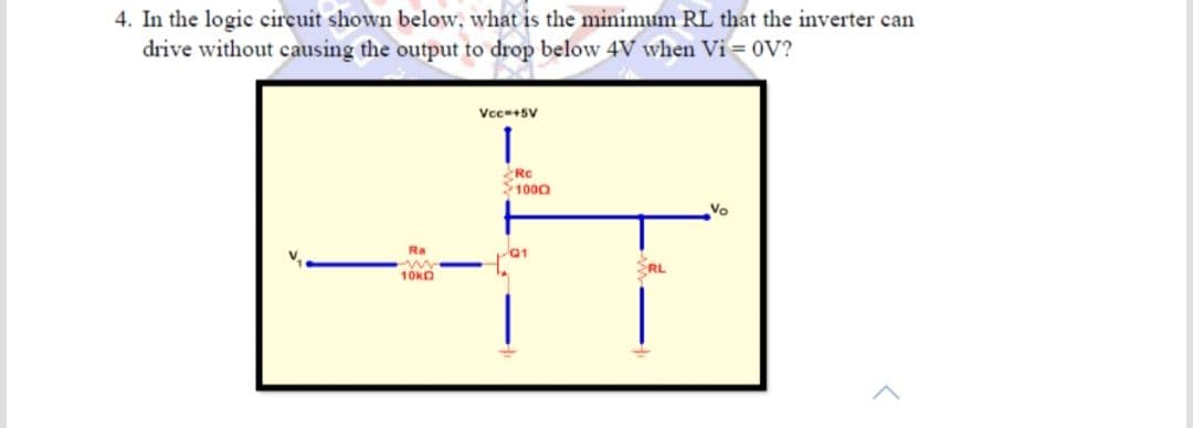
4. In the logic circuit shown below, what is the minimum RL that the inverter can drive without causing the output to drop below 4V when Vi = 0V? Vcc+SV 1000 Vo Ra 01 RL 10kO


Q: ülebäi The logic circuit represented by the figure shown below is A Doz B OR O AND O NAND O NOR O
A:
Q: 4. In the logic circuit shown below, what is the minimum RL that the inverter drive without causing…
A:
Q: A B 2
A: The given data is as follows:-
Q: Q2. а. Draw the equivalent purely NOR gate representation of the function (Used bubble method). F…
A: A Boolean expression is given in the question. We need to draw the equivalent purely NOR gate…
Q: Draw the logic diagram for the following functions, then map it using NAND only technology and NOR…
A:
Q: Realize the function f(a, b.c,d) = Em(13462.11.12.14) (Fonksiyonu gerçekleyiniz!) (a) Use a single…
A:
Q: Draw full circuit
A: Diagram of ECL implementation
Q: The logic swing in the inverter as shown is reducedby a factor of 3 by reducing the value of RCand…
A: Calculating collector resistance RC’ Calculating logic swing voltage
Q: Draw a logic diagram of a divide-by-14 counter using IC 7493 and 2-input AND gate.
A: We need to design a logic diagram of a divide-by-14 counter using IC 7493 and 2-input AND gate.…
Q: Design a three input NOR layout so that rise time and fall time become equal when input logic…
A: Given: A three-input NOR layout so that rise time and fall time become equal when input logic…
Q: ) (a) Find VH , V1 , and the power dissipation (for vo = V1 ) for the logic inverter with resistor…
A: Resistors are coupled to an inverter's DC bus circuit, consume motor regeneration power, and…
Q: 2. Use two AND gates, two NOR gates and one INVERTER to construct the D latch circuit shown in…
A: It is D latch which is modification of SR lstch In SR latch at s=1,R=1 output state is invalid so…
Q: Draw the logic diagram and transistor implementation for a (2-2-2) AOI.
A: The logic diagram can be implemented as,
Q: Q2. Minimize the combinational logic circuit in the following figure using Karnaugh's map only.…
A:
Q: Draw the logic circuit diagram using pure NAND gates and pure NOR gates: А В А ВСD Note: convert…
A: digital electronics problem.. Look below for the solution once...
Q: c) Explain the working of the circuit given in Figure 4 for inputs A =0 and B = 1. Give the value of…
A:
Q: QUESTION 1 True or False (correct the sentence if false): 1. An inverter performs a NOT operation.…
A: We are authorized to answer three subparts at a time, since you have not mentioned which part you…
Q: 2. Simplify the expression G = (X' + Y +Z') (W + X + Y + Z) (W' + X' + Y') using K- map and draw the…
A: Given : Note : In the given question first of all they want to know the answer for question number…
Q: Q2:Draw the logic circuit to Storage the data (110110).
A: As per the guideline we need to solve only first question. we need to draw the logic circuit to…
Q: Draw the logic diagram for the following functions, then map it using NAND only technology and NOR…
A: as per our company guidelines we are supposed to answer ?️only first 3️⃣ sub-parts. Kindly repost…
Q: Using the DC operating conditions from the following table, give the noise margin HIGH (NMH) for the…
A: Given that, VOHmax=2.4 VIHmin=2 A Noise margin is the amount of noise that CMOS can withstand…
Q: Doe Do Dor Do Vị V3 Figure 2: Simulating delays with inverters. Let each inverter have delay A, then…
A: Given the logic circuit as shown below: We need to construct this circuit using the MUX circuit. We…
Q: 6. Show that the circuit shown below functions as a logic inverter VDD Qi Vout Vin Q2
A: The explanation can be achieved as follow.
Q: A certain logic gate has a VOL(max) = 0.45 V, and it is driving a gate with a VIL(max) = 0.75 V. Are…
A: This question is from "Digital Electronics". Under which we are going to study the basic working…
Q: 2) Find VH, VL, and power dissipation (for vo = V1) for the logic inverter with saturated load in…
A:
Q: Five inverters are connected in series. Which of the following statements is correct? The output is…
A:
Q: 1- Implement the following function using NAND gates (Use the logic converter in EWB). F=…
A: According to the question, we need to implement the given function using NAND Gate.
Q: Draw the logic circuit for (a'+ b'+ c + d) (a+ b+ c'+ d) (a+ b'+ c +d) using NOR gates.
A: The solution is as follows.
Q: Use the results to simplify the logicexpression Z = ABC + ABC + ABC + ABC
A: As in the given equation, 3 input AND gate is used hence its Truth table is given as A B C Y 0…
Q: Due to availability of NAND gate ICs only, design a digital logic circuit for the following…
A:
Q: For the transistor in this question, assume Vpp= 1.8V, µCox= 600µAV1, HpCox= 200µAV*1, Vthl= 0.5 V,…
A: Given, VDD= 1.8V, UnCox= 600 microAV-1 , Vth=0.5v and UpCox= 200 microAV-1
Q: In the logic circuit shown below, what is the minimum RL that the inverter can drive without causing…
A: Given Vi = 0 V V0 = 4 V Vcc = 5 V Rc = 100
Q: Draw a logic diagram using only two-input NAND gates to implement the following expression: F=(AB +…
A:
Q: Draw and explain the operation in detail (while including necessary table) the block diagram and…
A:
Q: The circuit shown is that of a logic inverter. The electronic switch is closed (position x) if v, >…
A:
Q: Simplify the following logic expression by .using K-map (A + B)(A + C) إضافة ملف Implement the…
A:
Q: Given a Boolean function of a logic circuits: F = A·B+C•D Please answer the following question: 1)…
A:
Q: Find VH , VL , and the power dissipation (forvO = VL ) for the logic inverter with resistor load.…
A: Concept: A measure of the opposition to current flow in an electrical circuit is defined as…
Q: The circuit on the right consists of an inverter connected to a load. Suppose that the range of…
A: According to the question, we need to determine the restriction for load resistance for the given…
Q: 2- In the logic circuit shown below, what is the minimum R, that the inverter can drive without…
A:
Q: AB EXPERIMENT JAL 6. How many basic logic gates are required to construct a XOR gate? 1.4 2.5 3.6
A:
Q: Draw a logic gate circuit for the following functions: F = AB’ + C’(A + B) F = (X’Y+Z) + (X +YZ’)
A: (1) The function F = AB’ + C’(A + B) is implemented by using NOR gate, AND gate and OR gate.
Q: a) A standard TTL inverter gate is shown in the figure. The supply voltage is 5V. Calculate the…
A: Solution (a) - When Vi =0.1 V Thus, when the input voltage is 0.1 V than output voltage is 4.28 V.
Q: Design the logic circuit of a 3 to 8 line decoder with only NOR and NOTgates.
A:
Q: Draw the transistor schematic for the logic gate corresponding to the Euler paths above. Make sure…
A: CMOS is a gate which is consist of nMOS (Pull up network) and pMOS (pull down network).
Q: Implement the Logic expression using only NOT and two-input NAND gates. A+B+C+D
A:
Q: Z= (A+B + CDE)+ B CD
A: The function is given as, Z=A+B+C-DE-+B-CD-
Q: 9) A certain logic gate has a VOL(max) = 0.45 V, and it is driving a gate with a VIL(max) = 0.75 V.…
A: Given: A certain logic gate has VOL(max) = 0.45 V (Gate 1) VIL(max) = 0.75 V (driving gate) (Gate 2)…
Q: 4) Design a saturated-load gate that implements the logic function Y = A(B +C D) + E . base on the…
A: Logic gates- Logic gates are mathematical exponential process deals with true or false values…

Step by step
Solved in 2 steps with 2 images

- Draw the schematic for a four-input NOR gate witha saturated load device. What are the W/L ratios ofall the transistors, based on the reference inverter ? (b) What is VL if all the logic inputs are equal to 1?Which of the following is an important feature of the sum-of-products form of expressions? • The delay times are greatly reduced over other forms. • The maximum number of gates that any signal must pass through is reduced by a factor of two. • No signal must pass through more than 2 gates (not including inverters). • All logic circuits are reduced to nothing more than simple AND and OR gates.Design a 4-bit synchronous binary upcounter using T flip-flops. Draw only the logic diagram. Please show the process.
- Q1: Design a combinational circuit with four inputs lines that represent a decimal digit in BCD and four output lines that generate the 9’s complement of the input digit. Q: 2 Show how a full adder can be converted to full-subtractor with the addition of one inverter circuit.Simplify the expression G = (X’ + Y + Z’) (W + X + Y + Z) (W’ + X’ + Y’) using K- map and draw the corresponding simplified logic gate circuit.From the equation A' B C' + A B C D, draw the combinational minimised logic circuit using respective Logic gate symbols
- Find VH , VL , and the power dissipation (forvO = VL ) for the logic inverter with resistor load. (b) Repeat for . P6.37(b)Provide the correct answer and write a legible solution. 1. Simplify the expression F = ABCD + AB’CD + A’B’C’D using Karnaugh map method and draw the corresponding simplified logic gate circuit.Design a 2-bit synchronous binary counter using T flip-flops. Requirements: a.) State diagram b.) state table c.) State equation : A (t+1) = B (t+1) = d.) Flip-flop input functions : e.) Logic diagram
- Implement a 1-bit full adder circuit by using 4x1 MULTIPLEXER and an INVERTER. Data inputs are A, B, Cin and name the outputs as Sum, Cout.When Inverters are used as the input to a NAND gate, the circuit performs what logic function? When Inverters are used as the input to a NOR gate, the circuit performs what logic function? A point in a logic circuit labelled STB3 can assume which of the following states ? a.binary 0 b.binary 1 c.either binary 0 and 1Draw a logic gate circuit for the following functions: F = AB’ + C’(A + B) F = (X’Y+Z) + (X +YZ’)