
Videos
(a)
The small signal parameters for each of the transistor and the value of the composite transconductance for the given specifications.
(a)
Answer to Problem 11.80P
The value of the small signal parameters are
Explanation of Solution
Given:
The given diagram is shown in Figure 1
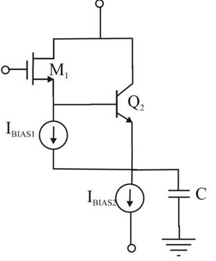
Figure 1
Calculation:
The expression to determine the value of the emitter current of the second transistor is calculated as,
The expression to determine the value of the current
Substitute
The value of the transconductance
The expression to determine the value of the small signal resistance is given by,
Substitute
The value of the drain current
The value of the transconductance
Substitute
The expression to determine the value of the composite transconductance is given by,
Substitute
Conclusion:
Therefore, the value of the small signal parameters are
(b)
The small signal parameters for each of the transistor and the value of the composite transconductance for the given specifications.
(b)
Answer to Problem 11.80P
The value of the small signal parameters are
Explanation of Solution
Given:
The given diagram is shown in Figure 1

Figure 1
Calculation:
The expression to determine the value of the emitter current of the second transistor is calculated as,
The expression to determine the value of the current
Substitute
The value of the transconductance
The expression to determine the value of the small signal resistance is given by,
Substitute
The value of the drain current
The value of the transconductance
Substitute
The expression to determine the value of the composite transconductance is given by,
Substitute
Conclusion:
Therefore, the value of the small signal parameters are
Want to see more full solutions like this?
Chapter 11 Solutions
Microelectronics Circuit Analysis and Design


- For the given circuit and the input waveform, answer the following questions: 1) Calculate the saturation current IC(sat). Then, for each time period of Vin waveform, calculate the value of VCE and determine the state of the transistor. Assume that: VCC = 12 V, RB = 5 kΩ, RC = 600 Ω, and VCE (sat) = 0.2 V. 2) Given that Vin = 2 V, and the transistor datasheet gives the following maximum ratings: PD(max) = 280 mW, VCE(max) =10 V, and IC(max) = 100 mA. Determine the maximum value to which VCC can be adjusted without exceeding a rating. Which rating will be exceeded first? Explain your answer.arrow_forward3. (a) The overall Noise Figure (NF) of a 2 –stage cascaded receiver is given as 35dB.The gain of the first stage is 4dB and the Noise Figure of the first stage is 28 dB.Find the noise figure and the equivalent noise temperature of the second stage.Assume the reference temperature is 17oC. (b) In a multi stage cascaded receiver, which stage mostly determines the overall NoiseFigure? Explain why. note: the answer will be by hand written.arrow_forwardIf the circuit of problem 2 is configured as a common-emitter amplifier, calculate the resulting voltage and current gain. Assume a load resistor of 1k ohm. Circuit of problem 2: determine the operating point of a universal trasnsistor DC bias cirucit when Vcc=15V, R1=10k ohm, R2=2.2k ohm, Rc=680 ohm, Re=100 ohm. Assume beta (b)=200 and Vbe=0.72V.arrow_forward
- In order to express the effect of the internal capacitors of BJT and the high frequency reception, the current gain expression depending on the frequency (Figure b) (hfe) is used in the case of collector emitter short circuit, voltage source connected at base end and emitter grounded (Figure la).. The catalog information of the 2N2222 transistor is given in Figure Ic. In the catalogue, when Ic=20 mA, it is seen as fT=250 MHz. a) Find the total capacitor effect for the case where gm> > wCμ. (Cpi) + (Cμ) = ?pFarrow_forwardThe LED in Figure below requires 30 mA to emit a sufficient level of light. Therefore, the collector current should be approximately 30 mA. For the following circuit values, determine the amplitude of the square wave input voltage necessary to make sure that the transistor saturates. Use double the minimum value of base current as a safety margin to ensure saturation. VCC = 8 V, VCE(sat) = 0.3 V, RC = 200 Ω , RB = 3.3 kΩ , b (beta) = 45, and VLED = 1.6 V.arrow_forwardWhat is the voltage gain of the common-emitter amplifier as shown? Assume βF = 135, VCC = VEE = 10 V, R1 = 20 kΩ, R2 = 62 kΩ,RC = 13 kΩ, and RE = 3.9 kΩ.arrow_forward
- SOLVE NUMBER 2 .1. Solve the output voltage if the gain is 24 db with aninput of 5mV.? 2. Assume a load resistor, RL of 2.2kΩs and a supply voltage of 24v. Calculate the Collector current (Ic) flowing through the load resistor when the transistor is switched fully "ON", assume Vce = 0, & β = 100. Also find the value of the Emitter resistor, Re with a voltage drop of 1.3v across it, R1, R2, and Ib. Assume also a value of 9 times Ib flowing through the resistor R2, while 10 times Ib flowing through R1.arrow_forwardFor a non -inverting operational amplifier, Rf = 80 kΩ , Ri = 6 kΩ fT = 2.35 MHz, Determine the closed loop lower critical frequency fc(cl) in kHzarrow_forwardAnswer all subparts In the circuit below the LED emits a sufficient light when saturated. Given that: VCC = 10 V, RC = 200 Ω, RB = 3.9 kΩ, βDC = 60, VCE (sat) = 0.2 V and VLED = 1.3 V. - Determine the minimum value of base current. - Determine the amplitude of the input voltage necessary to saturate the transistor. Use double the minimum value of base current as a safety margin to ensure saturation. - Determine the amplitude of the input voltage necessary to cut-off the transistor. - What is the main application when the transistor operation between cut-off and saturation?arrow_forward
- if the parameters for the BJT given Beta=120, VBE=0.7V, VT=26mV, VA=infinityarrow_forwardAnswer both A- Explain how to increase the efficiency of the solar cells (PV cells) through the integration of antennas. B- List three conditions need to be considered to choose a MOSFET for switching applications.arrow_forward4) By drawing the small signal model of the circuit given below, we can determine the total voltage and current gain values of the circuit, without the bypass capacitor on and without the bypass capacitor. Calculate separately for the two cases as it will be in the circuit (connected to the emitter end of the transistor). (β = 100, rS = 600 Ω, R1 = 27 KΩ, R2 = 4.7 KΩ, RC = 3.3 KΩ, RE = 680 Ω, RL= 15 KΩ, VCC = 10 V)arrow_forward
 Introductory Circuit Analysis (13th Edition)Electrical EngineeringISBN:9780133923605Author:Robert L. BoylestadPublisher:PEARSON
 Delmar's Standard Textbook Of ElectricityElectrical EngineeringISBN:9781337900348Author:Stephen L. HermanPublisher:Cengage Learning
 Programmable Logic ControllersElectrical EngineeringISBN:9780073373843Author:Frank D. PetruzellaPublisher:McGraw-Hill Education
 Fundamentals of Electric CircuitsElectrical EngineeringISBN:9780078028229Author:Charles K Alexander, Matthew SadikuPublisher:McGraw-Hill Education
 Electric Circuits. (11th Edition)Electrical EngineeringISBN:9780134746968Author:James W. Nilsson, Susan RiedelPublisher:PEARSON
 Engineering ElectromagneticsElectrical EngineeringISBN:9780078028151Author:Hayt, William H. (william Hart), Jr, BUCK, John A.Publisher:Mcgraw-hill Education,