
Concept explainers
Videos
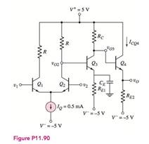
Consider the multistage bipolar circuit in Figure P 11.90, in which de base currents are negligible. Assume the transistor parameters are
(a)
The design parameters for the circuit.
Answer to Problem 11.90P
The value of the resistances to design the circuit is
Explanation of Solution
Given:
The given diagram is shown in Figure 1
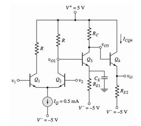
Figure 1
The given values are
Calculation:
The collector for both the transistors are equal and is given by,
The expression for the voltage
Substitute
The value of the voltage
The value of the resistance
The value of the resistance
The value of the resistance
Conclusion:
Therefore, the value of the resistances to design the circuit is
(b)
The value of the differential mode voltage gain
Answer to Problem 11.90P
The value of the differential voltage gain is
Explanation of Solution
The given diagram is shown in Figure 1

Figure 1
Calculation:
The expression for the gain
The value of the gain
The value of the resistance
The value of the gain
The value of the gain
The value of the voltage gain
Substitute
Conclusion:
Therefore, the value of the differential voltage gain is
(c)
The value of
Answer to Problem 11.90P
The values of the gain are
Explanation of Solution
The given diagram is shown in Figure 1

Figure 1
Calculation:
The value of the voltage
The value of the common mode voltage
Solve further as,
The value of the common mode rejection ration is calculated as,
Conclusion:
Therefore, the values of the gain are
Want to see more full solutions like this?
Chapter 11 Solutions
MICROELECT. CIRCUIT ANALYSIS&DESIGN (LL)


- Using the characteristic curve (please refer to the uploaded characteristic curve) of the NPN transistor of the class A Series - Fed Amplifier, shown in Figure 1 belowarrow_forwardFigure Q1(a) shows a Class A power amplifier circuit. Given the output signal is as shown in the figure, where Vm is the peak voltage and T is the period. For all transistors, you may neglect VBE and VCE(sat) in your calculations. (i) Derive an equation for power conversion efficiency, in terms of Vm, VCC, I and RL. Hence, deduce the maximum power conversion efficiency that is achievable. (ii) Determine the worst-case average power dissipation in each transistor under normal condition (i.e. RL is not open or short)arrow_forwardThe ac equivalent circuit for an amplifier is shown . Assume the capacitors have infinite value, RI = 750 Ω, RB = 100 kΩ, RC = 62 kΩ, and R3 = 100 kΩ. Calculate the voltage gain and input resistance for the amplifier if the BJT Q-point is (40μA, 10 V). Assume βo = 100 and VA = 75V.arrow_forward
- (a) Suppose υbe(t) = 0.005 sin 2000πt V in the bipolar amplifier as shown . Write expressions for υbe(t), vce(t), and υCE(t). (b) What is the maximum value of IC that corresponds to the active region of operation?arrow_forwardTopic: Field Effect Transistor Given the FET Amplifier circuit. Answer the question asked in each letter. a. Transconductance Gain (gm) b. Drain Resistor (RD) c. Input Impedance (Zi) d. Output Impedance (Zo) e. Voltage Gain (Av) f. What is the AC configuration of the amplifier?common source, common gate, common drain, or source bias?arrow_forwardDraw the equivalent circuit for a common-emitter bipolar transistor amplifier andderive suitable formulae for the amplifier current gain, voltage gain and power gain.Neglect bias,decoupling and coupling componentsarrow_forward
- write legible and show the complete process of solution topic(BJT Amplifiers)arrow_forwardIn the circuit given in the figure, Vcc = 15V, R1 = R2 = 10k ohm, RE = 1k ohm, RL = 0.5k ohm and transistor parameters are given as VBE = 0.7V, beta (dc) = beta (0) = 100. According to this;a) Calculate the values of DC bias currents and voltages (I (BQ), I (CQ), V (CEQ)).b) Using the hybrid model of the transistor, draw the small signal equivalent circuit of the circuit.c) Derive the input impedance expression of the circuit and calculate its value.d) Derive the voltage gain expressions A (vi) and A (VG) and calculate its value.e) Derive the current gain expression A (i) = I (0) / I (i) and calculate its value. I sent you question's image. Thank you..arrow_forwardQ.4/ Refer to the class AB power amplifier shown below:a. Determine the dc parameters VB(Q1), VB(Q2), ICQ, VCEQ(Q1), VCEQ(Q2).b. For the 5Vrms input, determine the power delivered to the load resistor.c. Determine the approximate input resistance seen by the signal source if ac=100arrow_forward
- Amplifier circuit is show below has a single ac input and one ac output. Assuming 2N2222 transistor: 1- Determine the Q point, then illustrate it on the transistor I-V characteristic curves. 2- Is the transistor in the active region? Explain thoroughly. 3- Construct the T-model of the transistor with all parameters labelled and evaluated. Assume room temperature. 4- Draw a complete small signal circuit model, then find the voltage gain. Explain two characteristics of this amplifier. 5- Calculate the current gain, the input resistance, and the output resistance.arrow_forwardFrom a cost standpoint, which system is more economical to install: a master amplifier distribution system or a multiset coupler? Explain the basic differences between these two systems. _______________arrow_forwardSince the transistors used in the circuit are B=100, ro=∞ a) Find the re1, re2 resistance values by performing the DC analysis for each amplifier stage separately. b) Draw the AC equivalent circuit of the amplifier circuit. c)Find the input and output impedance values for each amplifier stage. d) Find the voltage gains AV1, AV2 for each amplifier stage. e) Find the voltage value VL by finding the AV1 Voltage gain.arrow_forward
 EBK ELECTRICAL WIRING RESIDENTIALElectrical EngineeringISBN:9781337516549Author:SimmonsPublisher:CENGAGE LEARNING - CONSIGNMENT