
Videos
(a)
Value of current IDQ1 and ICQ2 .
(a)
Answer to Problem 12.40P
Value of current is,
Explanation of Solution
Given:
The given values are:
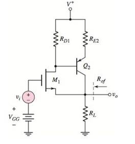
The given circuit is shown below.
Calculation:
Modified circuit diagram is shown below.
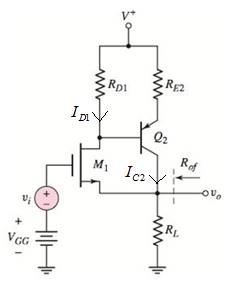
Neglecting base current.
Equation of current ID1 is,
Equation of voltage VD is,
Equation of current IC2 is,
Value of voltage VGS is,
Value of current IDQ1 is,
Value of current ICQ2 is,
(b)
Value of small signal voltage gain.
(b)
Answer to Problem 12.40P
Value of small signal voltage gain is 0.88.
Explanation of Solution
Given:
Given values are:
Calculation:
Small signal circuit is shown below.
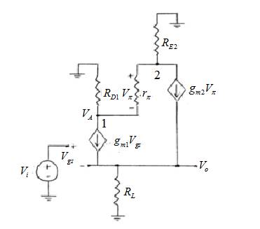
Value of trans-conductance of transistor 1 is,
Value of trans-conductance of transistor 2,
Value of small signal resistance is,
Applying KCL at node (2),
Equation of output voltage is,
Applying KCL at node (1),
Value of small signal voltage gain is,
(c)
Value of small signal output resistance.
(c)
Answer to Problem 12.40P
Value of small signal output resistance is
Explanation of Solution
Given:
Given values are,
Calculation:
Small signal circuit for output resistance calculation ( Vi =0) is,
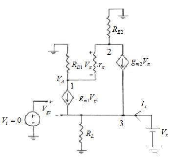
Applying KCL at node 3 for output resistance,
Want to see more full solutions like this?
Chapter 12 Solutions
Microelectronics Circuit Analysis and Design


- Bandwidth beta=250Hz, center frequency f0=750Hz of the band-proof circuit consisting of serial LCis desired.If the capacitor value is 100nF, what should the R and L values be?arrow_forwardWrite an expression for the loop gain of the active high-pass filter as shown.arrow_forwardFor the NMOSFET in the circuit below, K = 4.00mA/V^2, VTHN = 1.00V, l = 0V^-1, and VIN = 4.00V.a. Solve for IDS and VOUT and verify any assumptions you made. b. Derive an equation for the small signal gain of the circuit, vout / vin as a function of the vin radian frequency, w.arrow_forward
- IDSS=12mA , Vp=-8V , VGSQ=-2.4V , IDQ=4.12mA , Rsig=10kΩ , RG=100kΩ , RD=2,3kΩ , RS=470Ω , RL=39.7kΩ rD=20kΩ What is the volytage gain of the circuit? Note= FET output impedance rD=20kΩarrow_forwardFind 1)The value of midband voltage gain Avm = ..................... dB 2)The value of current gain AI = ................... 3)The value of Rin = ..................... 4)The value of fL due to C2 , fL2 = ..................... 5)The value of fH= .................. 6)The value of CE required to give fL = 200 Hz , CE = ............... 7)The slope of D.C.L.L = ......................... 8)The value of RE which makes the cct. bias-stable is RE = ................... 9)When CE is removed , the value of Av = ................. Electronics 2arrow_forwardA) Write the equation for the small-signal gain function ???????for the followingop-amp circuit B) What kind of filter is this circuit? C)Write the equation for the cutoff frequency of the filter D) Sketch the Frequency Response of the system.arrow_forward
- Q23) This multiple choice question from DIGITAL COMMUNICATIONS course.just write for me the final answer. A baseband system has a signal-to-noise ratio of 100 and a bandwidth efficiency of 1.25 .The average bit energy to noise spectral density of this system is equal to------- a)80 b)160 c)125 d)250arrow_forwardSketch the transfer curve defined by IDSS = 4 mA and VGS(off) = 3 V.arrow_forwardWrite a sample transfer function for a stable system with a closed cycle transfer function of 3rd degree.• According to this transfer function, the system is stable with the "Routh Hurwitz" method.arrow_forward
- 1. What is the order of the RC filter transfer function? 3rd 2nd 4th 1st 2. Why are unity gain amplifiers used? To separate complicated chains in signal transmission into separate simple circuits To filter the signal To amplify the signal To “condition the signal” so there is no voltage dividersarrow_forwardGiven the following: VCC = 15V C1= 1uFhfe =150 hie = 1.08 kΩR1 = 100kΩ C2 = 220uFR2 = 20 kΩ C3 = 0.32 uFRC = 2 kΩ Cwi = 12pF,Cwo = 10pF RE = 500 Ω Cbe = 15 pF Cbc = 25pFRL = 2 kΩ Determine the following: Midband gain Av Midband Total Voltage Gain AvT Midband Total Current Gain AiTarrow_forwardShort answer please. What are the main disadvantages of designing the band reject filter, mentioned above? Suggest a butter circuit design.arrow_forward
 Introductory Circuit Analysis (13th Edition)Electrical EngineeringISBN:9780133923605Author:Robert L. BoylestadPublisher:PEARSON
 Delmar's Standard Textbook Of ElectricityElectrical EngineeringISBN:9781337900348Author:Stephen L. HermanPublisher:Cengage Learning
 Programmable Logic ControllersElectrical EngineeringISBN:9780073373843Author:Frank D. PetruzellaPublisher:McGraw-Hill Education
 Fundamentals of Electric CircuitsElectrical EngineeringISBN:9780078028229Author:Charles K Alexander, Matthew SadikuPublisher:McGraw-Hill Education
 Electric Circuits. (11th Edition)Electrical EngineeringISBN:9780134746968Author:James W. Nilsson, Susan RiedelPublisher:PEARSON
 Engineering ElectromagneticsElectrical EngineeringISBN:9780078028151Author:Hayt, William H. (william Hart), Jr, BUCK, John A.Publisher:Mcgraw-hill Education,