
Videos
(a)
The value of the quiescent current
(a)
Answer to Problem 12.46P
The value of
Explanation of Solution
Given:
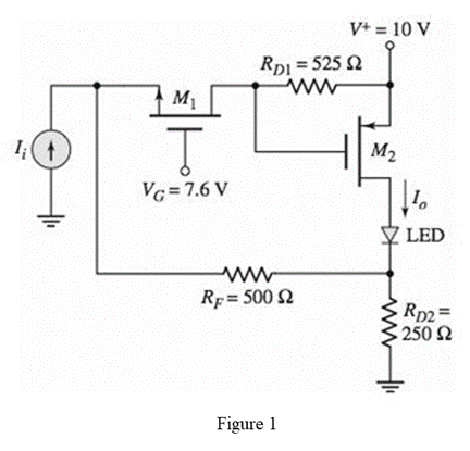
The given diagram is shown in Figure 1

Calculation:
The expression to determine the value of the voltage
The expression for the voltage
The expression for
The expression for the value of the gate to source voltage of the second transistor in terms of the second transistor drain current is given by,
Substitute
Substitute
The expression to determine the value of the gate voltage is given by,
Substitute
From trial and error method the value of the current
The expression for the value of the voltage
Substitute
Substitute
Substitute
Conclusion:
Therefore, the value of
(b)
To show: The expression for the small signal current gain is
(b)
Explanation of Solution
Given:
The given circuit is shown below.
Calculation:
The small signal equivalent circuit is shown in Figure 2
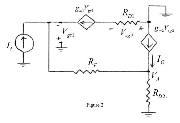
From above the expression for the output current is given by,
The expression for the voltage
Apply KCL at the upper left node.
The expression to determine the value of the
The expression for the value of the current at the output is given by,
Substitute
Substitute
Conclusion:
Therefore, the expression for the current gain is
(c)
The value of the current gain.
(c)
Answer to Problem 12.46P
The value of the current gain is
Explanation of Solution
Given:
The given diagram is shown in Figure 1

Calculation:
The expression to determine the value of the
Substitute
The expression to determine the value of the
Substitute
The expression for the current gain is given by,
Substitute
Conclusion:
Therefore, the value of the current gain is
Want to see more full solutions like this?
Chapter 12 Solutions
Microelectronics Circuit Analysis and Design


- Vs=100 mV peak-to-peak, 1 kHz sine signal, Kn=0.4mA/v^2 ,Vt=1V , λ=0.01V^-1 Make the DC analysis of the above given mosfet amplifier circuit. Simulation to tableWrite down the measured values and mathematical calculation results. (The valueswith the units.)DC Parameters ,Measured value ,Calculated ValueVGETCVGSVDVDSIDb. Draw the small signal model for the AC analysis of the circuit. Find the gm, ro, Av values.c. Show the Vs input signal and the Vo output signal of the circuit on the oscilloscope. Volt/div of channels andSpecify time/div values.arrow_forwardFor the feedback amplifier circuit shown below, assuming the internal resistor in each MOSFETs is infinite ( ro = ∞ ) and gm1 = gm2 = gm2 = 2.5mA/V. a) Draw the small AC equivalent circuit of the below amplifier. b) Determine the overall voltage gain.arrow_forwardIn the circuit given in the figure, Vcc = 15 V, R1 = R2 = 10kΩ, RE = 1KΩ, RL = 0.5kΩ and transistor parameters are given as VBE = 0.7V, ßdc = ß0 = 100. a. Calculate the values of DC bias currents and voltages (IBQ, ICQ and VCEQ). b. Draw the small signal equivalent circuit of the circuit using the hybrid model of the transistor. c. Derive the input impedance expression of the circuit and calculate its value. d. Derive the AVI and AVG voltage gain expressions and calculate their values. e. Derive the current gain expression AI = I0 / Ii and calculate its value. Compare this value you have calculated with the value you will calculate using the expression Aİ = Zi AVI / RL.arrow_forward
- Draw the midband small-signal equivalent circuit for the amplifier shown in FigureT12.5 . Be sure to label each element in your equivalent circuit.arrow_forwardThe ac equivalent circuit for an amplifier is shown. Assume the capacitors have infinite value, RI =750Ω, RB =100 kΩ, RC =100 kΩ, and R3 =100 kΩ. Calculate the input resistance and output resistance for the amplifier if the BJT Q-point is (75 μA, 10 V). Assume βo =100 and VA =75 V.arrow_forwardWrite an expression for the loop gain of the active low-pass filter as shown.arrow_forward
- Problem 1: Consider the circuit shown below. The transistor parameters are Kn1 = 0.5 mA/V2 , Kn2 = 0.2 mA/V2 , VT N1 = VT N2 = 1.2 V, and λ1 = λ2 = 0. The quiescent drain currents are ID1 = 0.2 mA and ID2 = 0.5 mA. (a) Determine the small-signal voltage gain of the given multistage amplifier. Answer: -6.14. (b) Calculate the small-signal output resistance Ro. Answer: 1.32 kΩ. Problem 2: The transistor parameters for the given circuit are β1 = 120, β2 = 80, VBE1 (on) = VBE2 (on) = 0.7 V, and VA1 = VA2 = ∞. (a) Determine the quiescent collector current in each transistor. Answer: IC1 = 2.253 mA, IC2 = 69.73 mA. (b) Find the small-signal voltage gain Av = vo/vs. Answer: 0.99. (c) Determine the input and output resistances Rib and Ro. Answer: Rib = 467.6 kΩ, Ro = 0.512 Ωarrow_forwardFor the 2 circuits shown above, βnpn = 100, βpnp = 50, VDO = 0.7 V, R2 = 150 kΩ, and RB = 12 kΩ Using the ac small-scale signal analysis, determine for each circuit: a) The voltage gain (Av = vout/vin) b) The input resistance (Rin) c) The output resistance (Rout)arrow_forwardThe ac equivalent circuit for an amplifier is shown . Assume the capacitors have infinite value, RI = 750 Ω, RB = 100 kΩ, RC = 62 kΩ, and R3 = 100 kΩ. Calculate the voltage gain and input resistance for the amplifier if the BJT Q-point is (40μA, 10 V). Assume βo = 100 and VA = 75V.arrow_forward
- 4. What is meant by Bandwidth of an amplifier?arrow_forwardThe circuit as shown is a shunt-shunt feedback amplifier. Use feedback analysis to find the midband input resistance, output resistance, and transresistance of the amplifier if RI = 500 Ω, RE = 2 kΩ, β0 = 100, VA = 50 V, RL = 5.6 kΩ, and RF = 47 kΩ, when vi and RI are replaced by a Norton equivalent circuit. What is the voltage gain for the circuit as drawn?arrow_forwardQ.4/ Refer to the class AB power amplifier shown below:a. Determine the dc parameters VB(Q1), VB(Q2), ICQ, VCEQ(Q1), VCEQ(Q2).b. For the 5Vrms input, determine the power delivered to the load resistor.c. Determine the approximate input resistance seen by the signal source if ac=100arrow_forward
 Power System Analysis and Design (MindTap Course ...Electrical EngineeringISBN:9781305632134Author:J. Duncan Glover, Thomas Overbye, Mulukutla S. SarmaPublisher:Cengage Learning