
Concept explainers
Videos
a.
Currents
a.
Answer to Problem 13.10P
Currents
Explanation of Solution
Given:
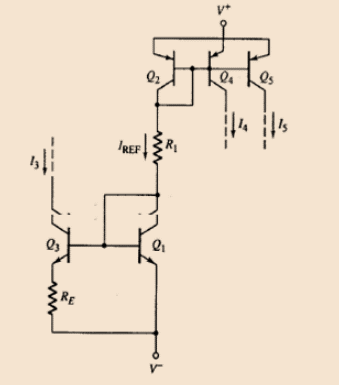
Circuit is given as;

Current for transistors
For
For
Reference current is given by,
Base to emitter voltage for any transistor is given by,
Therefore base to emitter voltage for transistor
Now, base to emitter voltage for transistor
Now putting the value of equation 2 and equation 3 in equation 1.
Using property of log equation 4 can be written as,
From the given data
Therefore,
Now putting the value of
Therefore reference current is equal to
Now,
Now putting all values,
Base to emitter voltage for transistor
As
Therefore from equation 2 and equation 4.
Now putting all values,
Base to emitter voltage for transistor
As
Therefore from equation 2 and equation 4.
Now putting all values,
b.
Currents
b.
Answer to Problem 13.10P
Currents
Explanation of Solution
Given:
Circuit is given as;
Current for transistors
For
For
Base to emitter voltage for transistor
As
Therefore from equation 2 and equation 4.
Now putting all values,
Base to emitter voltage for transistor
As
Therefore from equation 2 and equation 4.
Now putting all values,
Want to see more full solutions like this?
Chapter 13 Solutions
Microelectronics Circuit Analysis and Design


- The Type K thermocouple has a sensitivity of about 41 micro-Volts/℃, i.e. for each degree difference in the junction temperature, the output changes by 41 micro-Volts. Among 8-bit, 12-bit, 16-bit, 32-bit and 64-bit ADC, which is the most appropriate for measuring human body temperature to 4th decimal place (appropriate = accurate yet cost-effective), if the ADC range is 10 V?arrow_forwardDevelop the truth table and constellation diagram of QPSK using I -channel reference cos wct and 90 degrees phase shift for IQ inputs 00 and 10. Draw the analog output waveform of the given inputsarrow_forward3) For the given circuit;→Setup state thetransition table →Sketch state thesatate transitiondiagram→Derive the stateequationsarrow_forward
- answer all A - Explain the relation of MOSFET input current and input impedance and their effect on the functionality of the device. B- Explain how to increase the efficiency of the solar cells (PV cells) through the integration of antennas. C- List three conditions need to be considered to choose a MOSFET for switching applications.arrow_forwardAnswer as quickly as possible. I'll give upvote. Thank you. The circuit shown is a common source amplifier with a current mirror bias. It is given that the NMOS (M1) parameters are μoCox = 3mA/V2, VTH,n = 0.5V and λ = 0.02 and the PMOS (M2 and M3) parameters are μoCox = 1mA/V2 and VTH,p = −0.6V . The PMOS transistor M3 does not have channel length modulation while PMOS transistor M2 has λ = 0.02. It is also given that the dimensions of M2 and M3 have equal widths of 5µm and lengths of L2 = 3µm and L3 = 1.5µm, respectively. M1 has length of L1 = 1µm and width of W1 = 2µm. Find the gm and ro of transistor M1.arrow_forwardDetermine the folowing A.base current (IB), B. collector current (Ic), C. collector-to-emitter voltage (VCE),D. draw the load line, locate the Q-pointF. input impedance (Zi),G. Output impedance (Zo)arrow_forward
- The fixed- plus self-bias circuit of Figure 11.13 on page 569 has VDD = 15 V, R1 = 2 MΩ, R2 = 1 MΩ, RS = 4.7 kΩ, and RD=4.7 kΩ. The MOSFET has Vto = 1 V and K = 0.25 mA/V2. Determine the Q point.arrow_forwardProblem: Fx=(AB+CD+EF+G)' a. Draw its equivalent transistor circuit. b. Determine if the function has an Euler's path. please draw the equivalent Euler's path. C. Whether the circuit has a Euler's path or not, draw the stick diagram.arrow_forwardWhat is the term used to express the ability of a measuring system to maintain its standard performance? a) Zero Reliabilityb) Stabilityc) Sensitivityd) Linearityarrow_forward
- For the circuit shown, let VCC = 3.3 V, RE = 500 Ω, RC = 4 kΩ, R1 = 85 kΩ, R2 = 35 kΩ, and β = 150. Using approximation, determine the Q-point parameters: IBQ, ICQ, and VCEQ. Indicate the exact numerical values, following the given unit.arrow_forwardQ5 For the circuit shown, If the SCR shown is Continuously fired by a de Signal, Calculate the average Load Current ie 4Omega min V = 330Sin (314) Volt Ans : [a Amp E E = 165Uarrow_forwardVGSQ=6.8V , IDQ=2.4mA , VGS(Th)=3.3V , k=0,4x10⁻³A/V2 , RD=5.6kΩ , RF=2.2MΩ , rD=25kΩ . What is the voltage gain when RL = 15,6kΩ is connected the circuit? Note= MOSFET output resistance is taken into account in calculations.arrow_forward
 Introductory Circuit Analysis (13th Edition)Electrical EngineeringISBN:9780133923605Author:Robert L. BoylestadPublisher:PEARSON
 Delmar's Standard Textbook Of ElectricityElectrical EngineeringISBN:9781337900348Author:Stephen L. HermanPublisher:Cengage Learning
 Programmable Logic ControllersElectrical EngineeringISBN:9780073373843Author:Frank D. PetruzellaPublisher:McGraw-Hill Education
 Fundamentals of Electric CircuitsElectrical EngineeringISBN:9780078028229Author:Charles K Alexander, Matthew SadikuPublisher:McGraw-Hill Education
 Electric Circuits. (11th Edition)Electrical EngineeringISBN:9780134746968Author:James W. Nilsson, Susan RiedelPublisher:PEARSON
 Engineering ElectromagneticsElectrical EngineeringISBN:9780078028151Author:Hayt, William H. (william Hart), Jr, BUCK, John A.Publisher:Mcgraw-hill Education,