
Concept explainers
The currents
Answer to Problem 13.1EP
The currents are:
Explanation of Solution
Given:
The bias circuit and input stage portion of 741 op-amp circuit is shown below.
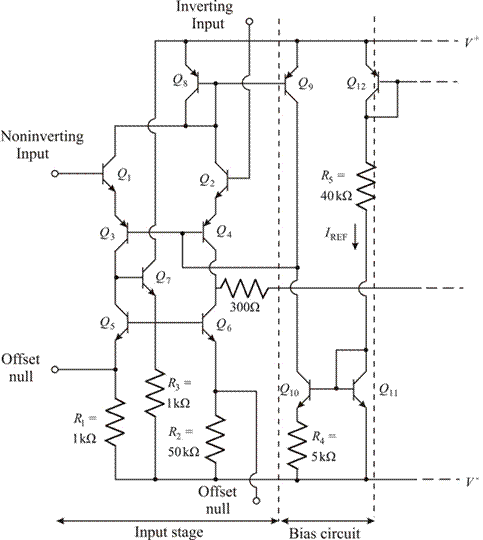
Figure 1
Resistance
Bias voltages are:
The base current is considered to be 0 A.
The base emitter voltages are:
Calculation:
Consider the given circuit. The formula for reference current that is established in the circuit branch consists of transistors
Transistors
Where,
Substitute the given values in the above equation.
By trial and error method,
For the given circuit, if the base current is neglected, then the collector current through transistors
Substituting the values,
Want to see more full solutions like this?
Chapter 13 Solutions
Microelectronics Circuit Analysis and Design


- Suppose we have a signal source with an internal (i.e., Thévenin) impedance that is always less than 1000 Ω, but is variable over time. Using the components listed in TableP13.36 , design an amplifier that produces an amplified version of the internal source voltage. The voltage gain should be −20±5 percent.arrow_forwardTrue or False Increasing RE improves the CMRR for single-ended output by increasing the differential-mode gain anddecreasing the common-mode gain. Increasing RE reduces the transistor DC currents and increases the DC output voltages. The double-ended output of the differential amplifier is always zero if vs1=vs2 for any value of RE.arrow_forwardFor the following differential amplifier below with, Vcc =15v, Re=100Ω, RE=100KΩ, Rc= 8KΩ, transistors with IE=1 mA and β=100. Calculate the Differential gain vod/vid. and input differential resistance.arrow_forward
- design and Draw the circuit of op-amp monostable multivibrator with fo= 200KHz and duty cycle of 40%arrow_forwardDesign a MOSFET differential pair which produces a differential output voltage of 2 V when (a) v1 =-90 mV and v2 = +90 mV (b) when one of the transistor grounded. The transistor parameters are Vtn =0.8 V, kn’(W/L) = 0.4 mA/V2 and λ=0. Choose the supply voltage to be ±10V with a constant currentsource of 5 mA. Also determine the maximum common mode input voltage.arrow_forward1. For an electronic device operating at a temperature of 17°C with a bandwidth of 10 kHz, determine:a. ThermalnoisepowerinwattsanddBm.b. Rmsnoisevoltagefora100Ωinternalresistance. 2. Two resistors, 20 kΩ and 50 kΩ are at ambient temperature. Calculate for a bandwidth equal to 100 kHz, the thermal noise voltage for the tworesistors connected in parallel.arrow_forward
- The ac equivalent circuit for an amplifier is shown. Assume the capacitors have infinite value, RI =750Ω, RB =100 kΩ, RC =100 kΩ, and R3 =100 kΩ. Calculate the input resistance and output resistance for the amplifier if the BJT Q-point is (75 μA, 10 V). Assume βo =100 and VA =75 V.arrow_forwardSlove Boperational amplifiers of your choice both FET and BJT based technology (make sure datasheets areavailable with your final report):A) From the datasheet, find the number of pins of the Op-amp IC, the open-loop gain,bandwidth, CMRR, slew rate, Voltage offset, current offset, input and output impedance,recommended supply voltages. Tabulate your outcomes with evidence from the data sheets.For both types of Op-Amps. Discus advantages and disadvantages of both.B) Mention available amplifiers that this op-amp is used for and discuss in brief itsapplications.arrow_forwardThe ac equivalent circuit for an amplifier is shown . Assume the capacitors have infinite value, RI = 10 kΩ, RB = 5 MΩ, RC = 1.5 MΩ, and R3 = 3.3 MΩ. Calculate the input resistance and output resistance for the amplifier if the BJT Q-point is (2 μA, 2 V). Assume βo = 40 and VA = 50 V.arrow_forward
- In the circuit in the figure, VGSQ = 6.8 V, IDQ = 2.4 mA, VGS(Th) = 3.3 V, k = 0.4x10⁻³ A/V2, RD = 5.6 kΩ, RF = 2.2 MΩ and rd = 25 kΩ. Accordingly, when a RL = 23.6 kΩ load is connected to the output of the circuit, what will be the voltage gain of the circuit? NOTE: MOSFET output resistance must be taken into account in rd calculations.arrow_forwardThe fixed- plus self-bias circuit of Figure 11.13 on page 569 has VDD = 15 V, R1 = 2 MΩ, R2 = 1 MΩ, RS = 4.7 kΩ, and RD=4.7 kΩ. The MOSFET has Vto = 1 V and K = 0.25 mA/V2. Determine the Q point.arrow_forwardMultiple Choice directions: Circle the letter of the answers that best answer the question. 13. When using microwave tubes as amplifiers, what is used as bandpass filters? a. Transistors b. Oscillator c. All of the above d. Power tubes 14. The microstrip lines used to achieve maximum power transfer are intended for a. Signal coupling b. Decoupling to prevent feedback c. Low-noise amplification d. Impedance matching and tuning 15. A diode that when reverse biased will momentarily and will abruptly turn off. a. Varactor diode b. IMPATT c. Step recovery diodes d. PIN diodes 16. A microwave transmission line used to minimize noise and crosstalks. a. Stripline b. Hard line cable c. Waveguide d. Microstrip 17. The major difference between a low frequency transistors and microwave types is/are. a. B & C b. Packaging c. Material d. Internal geometry 18. Which of the following band belongs to the millimeter waves a. C b. Ku c. U d. L 19. Overcrowding in the frequency spectrum is prevalent…arrow_forward
 Introductory Circuit Analysis (13th Edition)Electrical EngineeringISBN:9780133923605Author:Robert L. BoylestadPublisher:PEARSON
 Delmar's Standard Textbook Of ElectricityElectrical EngineeringISBN:9781337900348Author:Stephen L. HermanPublisher:Cengage Learning
 Programmable Logic ControllersElectrical EngineeringISBN:9780073373843Author:Frank D. PetruzellaPublisher:McGraw-Hill Education
 Fundamentals of Electric CircuitsElectrical EngineeringISBN:9780078028229Author:Charles K Alexander, Matthew SadikuPublisher:McGraw-Hill Education
 Electric Circuits. (11th Edition)Electrical EngineeringISBN:9780134746968Author:James W. Nilsson, Susan RiedelPublisher:PEARSON
 Engineering ElectromagneticsElectrical EngineeringISBN:9780078028151Author:Hayt, William H. (william Hart), Jr, BUCK, John A.Publisher:Mcgraw-hill Education,