
Videos
A.
Output voltage due to input bias current and worst case output voltage.
A.
Answer to Problem 14.50P
Output voltage due to input bias current is
Explanation of Solution
Given:
The given circuit is:
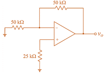
Input bias current
Input offset current
Let the general circuit with input bias currents
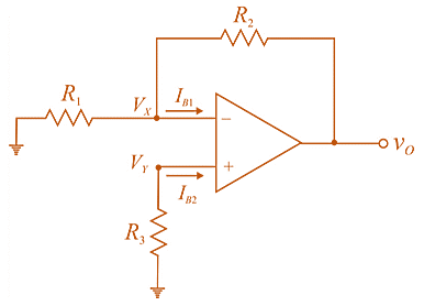
Now, using superposition determine
For
The output voltage due to
For
Since,
The output voltage due to
So, the vet output voltage due to both
If
So, the output voltage due to bias current
Now putting the values,
Now, for worst case output
As,
And
Adding (5) and (6)
From (5)
For
For
Assume
For the given circuit
Putting the values in (3)
So, including the effect of input offset current, the worst case output voltage is
B.
Output voltage due to input bias current and worst case output voltage.
B.
Answer to Problem 14.50P
Output voltage due to input bias current is
Explanation of Solution
Given:
The given circuit is:
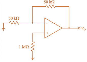
Input bias current
Input offset current
Considering equation 4.
Now, for worst case output voltage
Assume
For the given circuit
Putting the values in (3)
So, including the effect of input offset current, the worst case output voltage is
Want to see more full solutions like this?
Chapter 14 Solutions
Microelectronics Circuit Analysis and Design


- Find the following: DC gain, inductor current ripple and output voltage ripple: For DC-DC Buck converter: 1-Draw all circuits in all position 2-Sketch the transistor current waveform 3-Derive analytical expressions for the dc components of the capacitor voltages and inductor currents. 4-Derive analytical expressions for the peak ripple magnitudes of the input filter inductor current and capacitor voltage.arrow_forwardHow to tell the difference between a open loop transfer function and closed loop transfer function?arrow_forward1. (a) Define analog to digital converter (ADC). Draw a 4-bit ADC circuit using Op-Amps. (b) why modulations are used in AC telemetry.Draw and discuss a basic AC data telemetry system. Please ans both parts.arrow_forward
- a.Derive the excitation equations b. Determine transition and output equations c. Derive the transition/output table and Draw the state diagram.arrow_forwardFigure Q.4(c) shows a Schmitt Trigger circuit. Assuming that the output will saturate at ±Vsat = ±12 V and Vi = 8 sin wt [V],(i) Derive the expression for VUTP and VLTP.(ii) Draw and label the output signal, Vo.(iii) Draw and label the transfer characteristic, Vo vs Vi.arrow_forwardWhat is the output impedance of Common Emitter Collector Feedback preamplifier whose Collector Resistor is 2.7kohms, Feedback Resistor 180kohms?arrow_forward
- A resistive attenuator (e.g. coaxial cable) at room temperature has match input and output resistance and attenuation of L. Determine the equivalent temperature and noise figure of attenuator when the input source and attenuator are at room temperature. NOTE : in coaxial cable gain is 1/ attenuationarrow_forwardIn Steady-State Operation o f Buck DC-DC Converter Explain how the switching frequency component is eliminated by the output filter network.arrow_forwardI'm designing a mixer in Qucs. What does input frequency range and input voltage swing mean? Is it the AC voltage source's frequency and peak voltage?arrow_forward
- Consider the circuit of Figure 12.7 on page 605. Assume that VCC=20 V, VBB=0.3 V, RB=40 kΩ, and RC=2 kΩ. The input signal is a 0.2-V-peak 1-kHz sinusoid given by vin(t)=0.2 sin(2000πt). The common-emitter characteristics for the transistor are shown in Figure P12.18. Determine the maximum, minimum, and Q-point values for vCE. What is the approximate voltage gain for this circuit? Why is the gain so small in magnitude?arrow_forwardRouth Hurwitz analysis of closed loop system with variable gain.arrow_forwardBlock diagram reductionarrow_forward
 Power System Analysis and Design (MindTap Course ...Electrical EngineeringISBN:9781305632134Author:J. Duncan Glover, Thomas Overbye, Mulukutla S. SarmaPublisher:Cengage Learning
 Electricity for Refrigeration, Heating, and Air C...Mechanical EngineeringISBN:9781337399128Author:Russell E. SmithPublisher:Cengage Learning