Videos
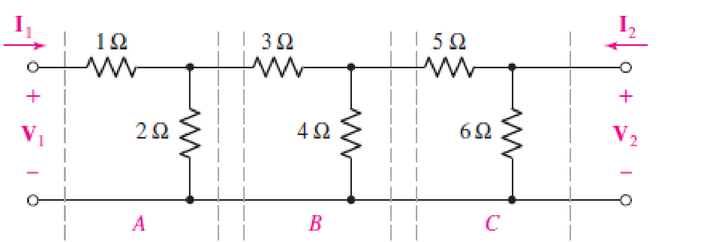
The two-port of Fig. 16.65 can be viewed as three separate cascaded two-ports A, B, and C. (a) Compute t for each network. (b) Obtain t for the cascaded network. (c) Verify your answer by naming the two middle nodes Vx and Vy, respectively, writing nodal equations, obtaining the admittance parameters from your nodal equations, and converting to t parameters using Table 16.1.
(a)
The
Answer to Problem 54E
The
Explanation of Solution
Calculation:
The required diagram is shown in Figure 1.
Here,
The mesh equation from the input side is given by,
The mesh equations at the output side is given by,
Substitute
The
Here,
Write equations (6) and (7) in matrix form.
Compare equation (3) with equation (4).
Compare equation (2) with equation (6).
The
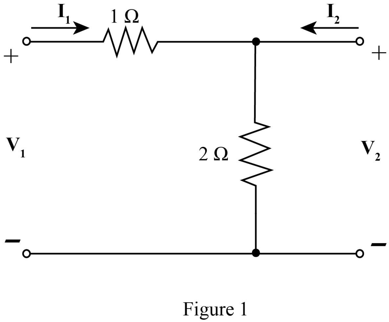
The required diagram is shown in Figure 2.
The mesh equation from the input side is given by,
The mesh equations at the output side is given by,
Substitute
Compare equation (8) with equation (4).
Compare equation (7) with equation (5).
The
The required diagram is shown in Figure 3.
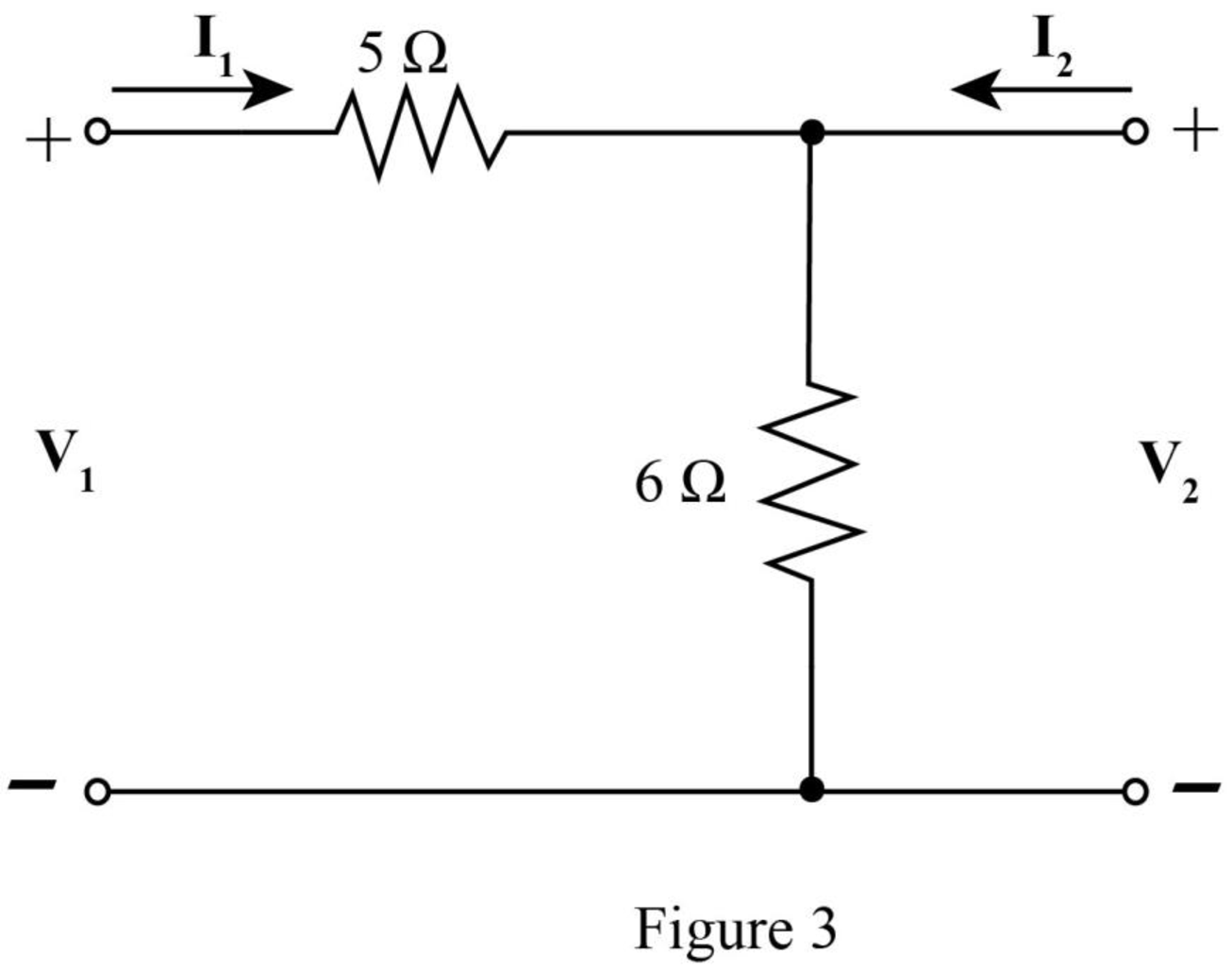
The mesh equation from the input side is given by,
The mesh equations at the output side is given by,
Substitute
Compare equation (11) with equation (4).
Compare equation (10) with equation (5).
The
Conclusion:
Therefore, the
(b)
The
Answer to Problem 54E
The
Explanation of Solution
Calculation:
The
Substitute
Conclusion:
Therefore, the
(c)
To verify: The above answers by obtaining the admittance parameter and converting them to
Answer to Problem 54E
The values have been verified.
Explanation of Solution
Calculation:
The required diagram is shown in Figure 4.
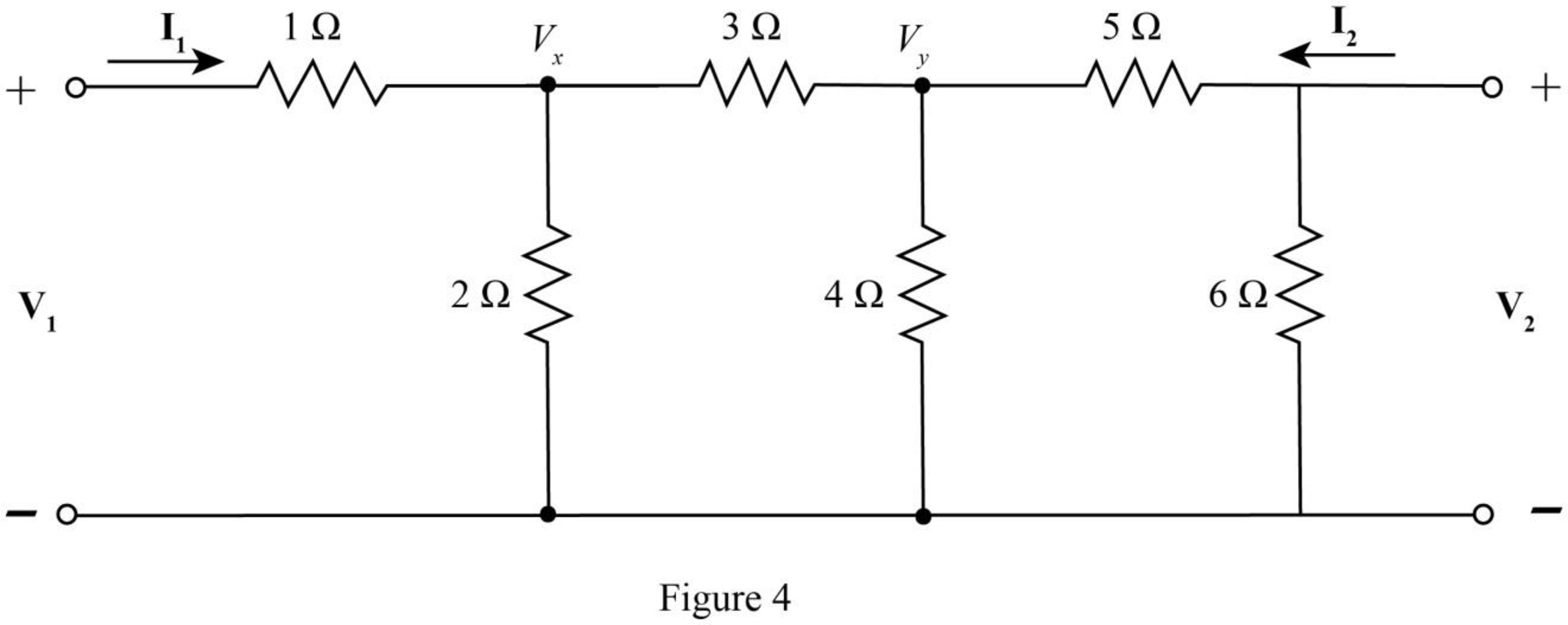
The nodal equation at node
The nodal equations at node
Substitute
Substitute
The current
Substitute
The current
Substitute
The
Here,
Compare equation (16) with equation (18).
Compare equation (17) with equation (19).
The determinant of the matrix
Substitute
The relation between
Substitute
Within the limits of error, the values have been verified.
Conclusion:
Therefore, the values have been verified.
Want to see more full solutions like this?
Chapter 16 Solutions
ENGINEERING CIRCUIT...(LL)>CUSTOM PKG.<
Additional Engineering Textbook Solutions
Electrical Engineering: Principles & Applications (7th Edition)
Engineering Electromagnetics
Fundamentals of Applied Electromagnetics (7th Edition)
Principles Of Electric Circuits
ANALYSIS+DESIGN OF LINEAR CIRCUITS(LL)
Fundamentals of Electric Circuits


- C. P = P, + USB + LSB eq 1 P = USB + LSB eq 2 After analyzing a modulation scheme, the above two results were obtained. As transmission engineer, you are to discuss the two expressions indicate which one will be preferred to the other and why your inclusion of the choice.arrow_forwardDetermine the Boolean expression that describes pull-down networks and pull-up networks. 1.) Y= A+B+ (CDE)arrow_forward1. Use 2's complement method to prove that (FA)16-(DC)16=(36), HASIN ALAM FDE 4212021arrow_forward
- 16.6 Design an output voltage-clamping circuit as shown in Fig. 16.14(a) so that the slope of the transfer char- acteristic is S = vo vs = 20, Vo(max) = 6.7 V, and Vo(min) = -8.7 V. Determine the zener voltages Vzı and Vz2. Assume Vp = 0.7 V. P + R₁ + Vd Vx + A = ∞ RF ZV22 Vz1 + VOarrow_forwardQ16/ a combinational circuit has four inputs (A, B, C, D), which represent a binary- coded- decimal digit. The circuit has two groups of four outputs S, T, U, V, and W, X, Y, Z each group represents a BCD digit. The output digits represent a decimal number which is five times the input number. For example if ABCD=D0111, the output are 0011 0101. ASsume that invalid BCD digits do not occur as inputs. a- Construct the truth table b- Write minterms and max terms for all output C- Find SOP and POS for all outputarrow_forwardi) 1. For the Boolean function, Z = A + B +H(C+DF) + EG Draw the schematic of the pull-up and pull-down networks, Determine the equivalent width of the pull-down network if the width of each transistor at the network is W₁ = 2μm. ii)arrow_forward
- 16.8 Find the Z parameters for the two-port network in Fig. P16.8. I1 21 N I2 V1 42 0 10.5 V2 Figure P16.8arrow_forwarddigital ckts. Q.2. Realize the following functions using minimum number of components to draw their digital circuits. 1. AB+ABAB 2 ABC + ABE + ABC 3. (A + B) (A + B) 4. (A+B+C). (A + 5 + c) (A + 3+C)arrow_forwardi) Convert (ED23)16 to Octal (ii) Using 16’s complement representation; perform subtraction X-Y and Y-XWhere X= 10111100Y=10101011arrow_forward
 Introductory Circuit Analysis (13th Edition)Electrical EngineeringISBN:9780133923605Author:Robert L. BoylestadPublisher:PEARSON
 Delmar's Standard Textbook Of ElectricityElectrical EngineeringISBN:9781337900348Author:Stephen L. HermanPublisher:Cengage Learning
 Programmable Logic ControllersElectrical EngineeringISBN:9780073373843Author:Frank D. PetruzellaPublisher:McGraw-Hill Education
 Fundamentals of Electric CircuitsElectrical EngineeringISBN:9780078028229Author:Charles K Alexander, Matthew SadikuPublisher:McGraw-Hill Education
 Electric Circuits. (11th Edition)Electrical EngineeringISBN:9780134746968Author:James W. Nilsson, Susan RiedelPublisher:PEARSON
 Engineering ElectromagneticsElectrical EngineeringISBN:9780078028151Author:Hayt, William H. (william Hart), Jr, BUCK, John A.Publisher:Mcgraw-hill Education,