
Videos
The parameters of the TIL NAND circuit in Figure 17.24 are:
(a)
The value of the base and the collector current in each of the transistor.
Answer to Problem 17.9EP
The value of the currents are
Explanation of Solution
Calculation:
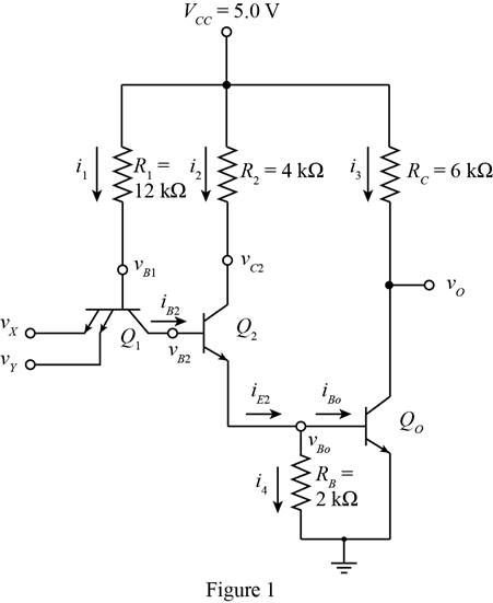
The given diagram is shown in Figure 1.
The expression for the voltage
Substitute
The second transistor and the transistor at the output are both cut off, then the base voltage
Substitute
The expression for the value of the current
Substitute
The expression to determine the value of the base current
Substitute
The transistor two and the output transistor are cutoff, therefore the value of the current are given by,
The expression for the value of the current
Conclusion:
Therefore, the value of the currents are
(b)
The value of the base and the collector current in each of the transistor.
Answer to Problem 17.9EP
The value of the currents are
Explanation of Solution
Calculation:
The input transistor is biased with inverse active mode when the input voltage is
The expression for the voltage
Substitute
The expression to determine the value of the collector voltage is given by,
Substitute
The expression to determine the value of the current
Substitute
The expression to determine the value of the base current
Substitute
The expression to determine the value of the current
Substitute
The expression to determine the value of the collector current
Substitute
The expression to determine the value of the current
Substitute
The expression to determine the value of the base current
Substitute
The expression to determine the value of the base current
Substitute
The expression to determine the value of the current
Substitute
The expression to determine the value of the current
Substitute
The expression to determine the value of the current
Substitute
Conclusion:
Therefore, the value of the currents are
Want to see more full solutions like this?
Chapter 17 Solutions
MICROELECT. CIRCUIT ANALYSIS&DESIGN (LL)


- (1) The bandwidth of the input signal is 4 MHz. The PCM encoder uses 256 quantization levels. What is the date rate of the PCM encoder? (2) What is the data rate then of a Delta Modulation encoder that uses the same sampling rate as that of the PCM encoder? (3) What is the resulting SNR in (1)?arrow_forwardDraw the schematic of a three-input NAND gate. What are the W/L ratios for thetransistors based?arrow_forward2/ a communications channel of 5 MHz. Determine the maximum transmission rate possible with an 8-PSK modulator considering a unit fall factor (R = 1). Compare it with the Maximum transmission rate of a QPSK modulator with the same fall factor. Which Modulator would you recommend and why?arrow_forward
- IV (a) If R = 25 Kohm and C = 12 uF, find the frequency of the astable multivibrator using NAND gate? Draw the diagram and its output waveform for Vcc = + 15 V. (b) If C=9nF, the frequency F=72KHz of the Monostable multivibrator using NAND gate . Find the value of resistance ?arrow_forward15. How many OC signals are used in a SONET network with a 622.08 Mbps line rate?A. 8064B. 4C. 12D. 8arrow_forwardDraw the circuit schematic of a three-input NANDgate. Suppose the NMOS transistors are chosen tohave (W/L)N =2/1. What are the correspondingW/L ratios of the PMOS devices, if the gate is tohave symmetrical delay characteristics?arrow_forward
- Draw and show the BFSK modulation waveform for the given binary data sequence “1,0,0,1”, and also draw its BFSK constellation diagram.arrow_forwardEstimate the gate capacitance of PMOS transistor (? = 0.36?, ? =0.18?). Gate oxide thickness is 40Å . Relative permittivity of silicon dioxide is 3.9. Vacuumpermittivity ?0 = 8.854 ? 10−12F·?−1. Answer in fF , round off to 4 decimal places.arrow_forwardFind the BER of a 64-QAM system with SNR=10 dB. NOTE: Use Q-function table as needed.arrow_forward
- Sketch the Bipolar RZ Voltage encoding on a classic Ethernet for the bit stream0001110101.arrow_forward4/ For a QPSK modulator with a 10 Mbps transmission rate and a carrier frequency 70 kHz. Consider a high cosine pulse with r = 0.5. (1 A/ Determine the minimum transmission bandwidth B/ Determine the wide width of a BPSK modulator with the same data transmission rate and the same type of pulse.arrow_forwardThe common-emitter output characteristics for annpn transistor are given . What are thevalues of βF at (a) IC = 5 mA and VC E = 5 V?(b) IC = 7 mA and VC E = 7.5 V? (c) IC = 10 mAand VC E = 14 V?arrow_forward
 Introductory Circuit Analysis (13th Edition)Electrical EngineeringISBN:9780133923605Author:Robert L. BoylestadPublisher:PEARSON
 Delmar's Standard Textbook Of ElectricityElectrical EngineeringISBN:9781337900348Author:Stephen L. HermanPublisher:Cengage Learning
 Programmable Logic ControllersElectrical EngineeringISBN:9780073373843Author:Frank D. PetruzellaPublisher:McGraw-Hill Education
 Fundamentals of Electric CircuitsElectrical EngineeringISBN:9780078028229Author:Charles K Alexander, Matthew SadikuPublisher:McGraw-Hill Education
 Electric Circuits. (11th Edition)Electrical EngineeringISBN:9780134746968Author:James W. Nilsson, Susan RiedelPublisher:PEARSON
 Engineering ElectromagneticsElectrical EngineeringISBN:9780078028151Author:Hayt, William H. (william Hart), Jr, BUCK, John A.Publisher:Mcgraw-hill Education,