
INTRO.TO COMPUTING SYSTEMS >INTL.ED.<
3rd Edition
ISBN: 9781260565911
Author: PATT
Publisher: MCG
expand_more
expand_more
format_list_bulleted
Videos
Textbook Question
Chapter 4, Problem 19E
Shown below is a byte-addressible memory consisting of eight locations, and its associated MAR and MDR. Both MAR and MDR consist of flip-flops that are latched at the start of each clock cycle based on the values on their corresponding input lines. A memory read is initiated every cycle, and the data is available by the end of that cycle.
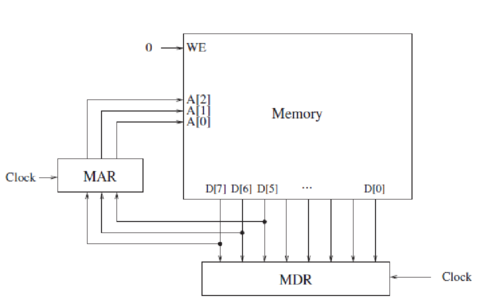
Just before the start of cycle 1, MAR contains 000, MDR contains 00010101, and the contents of each memory location is as shown.

a. What do MAR and MDR contain just before the end of cycle 1?
MAR:  MDR:
MDR: 
b. What does MDR contain just before the end of cycle 4?
MDR: 
Expert Solution & Answer
Want to see the full answer?
Check out a sample textbook solution
Students have asked these similar questions
In a dynamic random access memory (DRAM) computer chip, each memory cell chiefly consists of a capacitor for charge storage. Each of these cells represents a single binary-bit value of 1 when its 35-fFfcapacitor (1fF=10^−15F) is charged at 1.5 V, or 0 when uncharged at 0 V.
A)When it is fully charged, how many excess electrons are on a cell capacitor's negative plate?
B)
After charge has been placed on a cell capacitor's plate, it slowly "leaks" off (through a variety of mechanisms) at a constant rate of 0.30 fC/s. How long does it take for the potential difference across this capacitor to decrease by 1.0% from its fully charged value? (Because of this leakage effect, the charge on a DRAM capacitor is "refreshed" many times per second.)
Express your answer to two significant figures and include the appropriate units.
D-Latch is a simple clocked memory element in which the output is equal to the stored state inside the element.
In D-Latch the state is changed whenever the appropriate inputs change and the clock is asserted. A D-Latch has two inputs and two outputs.
The inputs are the data value to be stored and a clock signal that indicates when the latch should read the value on the data input and store it. The outputs are simply the value of the internal state and its complement.
When the clock input is asserted, the latch is said to be open, and the value of the output becomes the value of the data input. When the clock input is de-asserted, the latch is said to be closed, and the value of the output is whatever value was stored the last time the latch was open.
What is the difference between DFF and D-Latch?
Can one chip be used for constructing the other? Explain.
A digital computer has a memory unit with 24 bits per word. The instruction set consists of 150 different operations. All instructions have an operation code part (opcode) and an address part (allowing for only one address). Each instruction is stored in one word of memory.Q.) What is the maximum allowable size for memory?
Chapter 4 Solutions
INTRO.TO COMPUTING SYSTEMS >INTL.ED.<
Ch. 4 - Prob. 1ECh. 4 - Prob. 2ECh. 4 - What is misleading about the name program counter?...Ch. 4 - Prob. 4ECh. 4 - Prob. 5ECh. 4 - What are the two components of an instruction?...Ch. 4 - Prob. 7ECh. 4 - The FETCH phase of the instruction cycle does two...Ch. 4 - Prob. 10ECh. 4 - State the phases of the instruction cycle, and...
Knowledge Booster


Learn more about
Need a deep-dive on the concept behind this application? Look no further. Learn more about this topic, computer-science and related others by exploring similar questions and additional content below.Similar questions
- A computer system contains a big endian byte addressable memory system with 8 separate memory modules. Each memory module is 32 bits wide and contains 134217728 cells. Cells within each memory module are numbered 0 through 134217727. a) If the memory employs high order interleaving, what is the 32-bit memory address of cell 1048578 within module 3? b) If the high order interleaved memory uses little-endian instead of big-endian storage order, what is the 32-bit memory address of cell 511 within module 1? c) If the memory employs low order interleaving, what is the 32-bit memory address of byte 1048575 within module 2? Bytes are numbered starting from 0. Express the address in hex. d) What is the main advantage of using low-order interleaved memory compared to using high-order interleaved memory?arrow_forwardQ2- Write a program in assembly language for the 8085 microprocessor to receive one byte of data via the SID and store it at the memory address (3000H to 3009H) using a baud rate of 1200. Information: The 8085 processor operates at a frequency of 3.072 MHz . When receive the required bytes, you must adhere to the following: The bits of two high bits will be received at the beginning of the reception(start bits 1 1 ), after that the data bits will be received, after that the low bit of the stop bit will be received (stop bit 0 ). The following flowchart will help you. The solution must be integrated and include the calculation of the baudrate delay timearrow_forward4arrow_forward
- Q1- Write a program in assembly language for the 8085 microprocessor to receive 10 bytes of data via the SID and store it at the memory address (3000H to 3009H) using a baud rate of 1200. Information: The 8085 processor operates at a frequency of 3.072 MHz. When you receive each byte of the required bytes, you must adhere to the following: The bits of two high bits will be received at the beginning of the reception (start bits), after that the data bits will be received, after that the low bit of the stop bit will be received (stop bit). The following flowchart will help you, but you should notice that this flowchart deals with one byte, and you are required to deal with 10 bytes The solution must be integrated and include the calculation of the baudrate delay time Of+CD!HID+[00 Yes SIDATA Read SID Start Bit? Wait for Half-Bit Time Set up Bit Counter Wait Bit Time Read SID Save Bit Decrement Bit Counter All Bits Received? Add Bit to Previous Bits Go Back to Get Next Bit Return IMUNIarrow_forwardThe 32-bit number 52AB43FC (in hexadecimal) is stored in abyte-addressable memory starting at physical address FE08 (in hex) using Little-Endian notation. The byte(value ni hexadecimal) stored at theaddress FE0B will bearrow_forwardA digital computer has a memory unit with 24 bits per word. The instruction set consists of 150 different operations. All instructions have an operation code part (opcode) and an address part (allowing for only one address). Each instruction is stored in one word of memory.Q.) What is the largest unsigned binary number that can be accommodated in one word of memory?arrow_forward
- The machines that use MISD are systolic arrays. A systolic array is a "wavefront" or data processing pipeline. Because data triggers execution, these sections don't need programme counters and may function independently. When all of the clocks in a systolic array are synchronized, the CPUs are able to do calculations in what is called "lock-step."arrow_forwardShow how the decimal value 2019111310 would be stored by byte-addressable machines with 32-bit words, using little endian format and then big endian format. Assume the value starts at address 201916. Draw a diagram of memory and place the appropriate values in the correct (and labeled) memory locations.arrow_forwardPlease help me with this Computer science homeworkarrow_forward
- Consider memory storage of a 32-bit word stored at memory word 34 in a byte addressable memory. (a) What is the byte address of memory word 34? (b) What are the byte addresses that memory word 34 spans? (c) Draw the number 0x3F526372 stored at word 342 in both big-endian and little-endian machines. Clearly label the byte address corresponding to each data byte value.arrow_forwardFigure 1 shows the design of a 6116 static CMOS RAM that can store 2K bytes of data. The memory has 16384 cells, arranged as a 128X128 memory matrix. The 11 address lines, which are needed to address 211 bytes of data, are divided into two groups. Lines A10 through A4 select one of the 128 rows in the matrix. Lines A3 through A0 select 8 columns in the matrix at a time since there are 8 data lines. The data outputs from the matrix go through tri-state buffers before connecting to the data I/O lines. These buffers are disabled except when reading from the memory. Table 1 shows the truth table of the SRAM block. Model the 6116 SRAM block using VHDL. You should incorporate the timing specifications of the 6116 block in your VHDL model by looking at its datasheet. A10 Memory Matrix Row Decoder 128 X 128 A4 ... 107 Column I/0 Input Data Column Decoder Control A3 A2 A1 Ao OE D WE CS Figure 1. Table 1. CS OE WE Mode /0 pins X Not selected High-Z High-Z Data out X Output disabled Read Write L…arrow_forwardA computer system interfaces a memory with a 32-bit address bus and a 16-bit data bus. The memory addressing is performed using a decoder. What is the number of AND gates needed to implement the decoder? What is the FAN OUT of the decoder?arrow_forward
arrow_back_ios
SEE MORE QUESTIONS
arrow_forward_ios
Recommended textbooks for you
 Systems ArchitectureComputer ScienceISBN:9781305080195Author:Stephen D. BurdPublisher:Cengage Learning
Systems Architecture
Computer Science
ISBN:9781305080195
Author:Stephen D. Burd
Publisher:Cengage Learning
Instruction Format (With reference to address); Author: ChiragBhalodia;https://www.youtube.com/watch?v=lNdy8HREvgo;License: Standard YouTube License, CC-BY