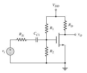
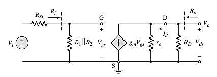
Problem 4.1EP Problem 4.2EP: For the circuit shown in Figure 4.1, VDD=3.3V and RD=10k . The transistor parameters are VTN=0.4V ,... Problem 4.1TYU Problem 4.2TYU: For the circuit shown in Figure 4.1, VDD=3.3V and RD=8k . The transistor parameters are VTN=0.4V ,... Problem 4.3TYU: For the circuit in Figure 4.1, the circuit and transistor parameters are given in Exercise TYU 4.2.... Problem 4.4TYU: The parameters for the circuit in Figure 4.8 are VDD=5V and RD=5k . The transistor parameters are... Problem 4.5TYU: A transistor has the same parameters as those given in Exercise Ex4.1. In addition, the body effect... Problem 4.3EP: The parameters of the circuit shown in Figure 4.14 are VDD=5V , R1=520k , R2=320k , RD=10k , and... Problem 4.4EP: Consider the circuit shown in Figure 4.14. Assume transistor parameters of VTN=0.8V , Kn=0.20mA/V2 ,... Problem 4.5EP: For the circuit shown in Figure 4.19, the transistor parameters are VTN=0.8V , Kn=1mA/V2 and =0 .... Problem 4.6EP: The commonsource amplifier in Figure 4.23 has transistor parameters kp=40A/V2 , W/L=40 , VTP=0.4V ,... Problem 4.6TYU: Consider the commonsource amplifier in Figure 4.24 with transistor parameters VTN=1.8V ,... Problem 4.7TYU: The parameters of the transistor shown in Figure 4.25 are: VTP=+0.8V , Kp=0.5mA/V2 , and =0.02V1 .... Problem 4.7EP: The sourcefollower circuit in Figure 4.26 has transistor parameters VTN=+0.8V , Kn=1mA/V2 , and... Problem 4.8EP: The circuit and transistor parameters for the sourcefollower amplifier shown in Figure 4.29 are... Problem 4.9EP: Consider the circuit shown in Figure 4.28 with circuit parameters VDD=5V , RS=5k , R1=70.7k ,... Problem 4.8TYU Problem 4.9TYU: The transistor in the sourcefollower circuit shown in Figure 4.31 is biased with a constant current... Problem 4.10EP: Consider the circuit shown in Figure 4.35 with circuit parameters V+=5V , V=5V , RS=4k , RD=2k ,... Problem 4.10TYU: For the circuit shown in Figure 4.32, the circuit parameters are: V+=5V , V=5V , RG=100k , RL=4k ,... Problem 4.11EP: The bias voltage for the enhancementload amplifier shown in Figure 4.39(a) is VDD=3.3V . The... Problem 4.12EP: Assume the depletionload amplifier in Figure 4.43(a) is biased at IDQ=0.1mA . The transistor... Problem 4.13EP: For the circuit shown in Figure 4.45(a), assume transistor parameters of VTN=+0.5V , VTP=0.5V ,... Problem 4.14EP: The transconductance gm of the transistor in the circuit of Figure 4.47 is to be changed by changing... Problem 4.15EP: The transconductance gm of the transistor in the circuit of Figure 4.48 is to be changed by changing... Problem 4.11TYU: For the enhancement load amplifier shown in Figure 4.39(a), the parameters are: VTND=VTNL=0.8V ,... Problem 4.16EP: For the cascade circuit shown in Figure 4.49, the transistor and circuit parameters are given in... Problem 4.17EP: The transistor parameters of the NMOS cascode circuit in Figure 4.51 are VTN1=VTN2=0.8V ,... Problem 4.12TYU: The transistor parameters of the circuit in Figure 4.49 are VTN1=VTN2=0.6V , Kn1=1.5mA/V2 ,... Problem 4.19EP: Reconsider the sourcefollower circuit shown in Figure 4.57 with transistor parameters IDSS=8mA ,... Problem 4.13TYU Problem 4.14TYU: For the circuit shown in Figure 4.59, the transistor parameters are: IDSS=6mA , |VP|=2V , and =0 .... Problem 1RQ: Discuss, using the concept of a load line, how a simple commonsource circuit can amplify a... Problem 2RQ: How does the transistor widthtolength ratio affect the smallsignal voltage gain of a commonsource... Problem 3RQ: Discuss the physical meaning of the smallsignal circuit parameter ro . Problem 4RQ Problem 5RQ Problem 6RQ: Discuss the general conditions under which a commonsource amplifier would be used. Problem 7RQ: Why, in general, is the magnitude of the voltage gain of a commonsource amplifier relatively small? Problem 8RQ: What are the changes in dc and ac characteristics of a commonsource amplifier when a source resistor... Problem 9RQ: Sketch a simple sourcefollower amplifier circuit and discuss the general ac circuit characteristics... Problem 10RQ: Sketch a simple commongate amplifier circuit and discuss the general ac circuit characteristics... Problem 11RQ Problem 12RQ Problem 13RQ: State the advantage of using transistors in place of resistors in MOSFET integrated circuits. Problem 14RQ Problem 4.1P: An NMOS transistor has parameters VTN=0.4V , kn=100A/V2 , and =0.02V1 . (a) (i) Determine the... Problem 4.2P: A PMOS transistor has parameters VTP=0.6V , kp=40A/V2 , and =0.015V1 . (a) (i) Determine the... Problem 4.3P: An NMOS transistor is biased in the saturation region at a constant VGS . The drain current is... Problem 4.4P: The minimum value of smallsignal resistance of a PMOS transistor is to be ro=100k . If =0.012V1 ,... Problem 4.5P: An nchannel MOSFET is biased in the saturation region at a constant VGS . (a) The drain current is... Problem 4.6P: The value of for a MOSFET is 0.02V1 . (a) What is the value of ro at (i) ID=50A and at (ii) ID=500A... Problem 4.7P Problem 4.8P: The parameters of the circuit in Figure 4.1 are VDD=3.3V and RD=5k . The transistor parameters are... Problem 4.9P: The circuit shown in Figure 4.1 has parameters VDD=2.5V and RD=10k . The transistor is biased at... Problem 4.10P: For the circuit shown in Figure 4.1, the transistor parameters are VTN=0.6V , kn=80A/V2 , and... Problem 4.11P: In our analyses, we assumed the smallsignal condition given by Equation (4.4). Now consider Equation... Problem 4.12P: Using the results of Problem 4.11, find the peak amplitude Vgs that produces a secondharmonic... Problem 4.13P: Consider the circuit in Figure 4.14 in the text. The circuit parameters are VDD=3.3V , RD=8k ,... Problem 4.14P: A commonsource amplifier, such as shown in Figure 4.14 in the text, has parameters ro=100k and RD=5k... Problem 4.15P: For the NMOS commonsource amplifier in Figure P4.15, the transistor parameters are: VTN=0.8V ,... Problem 4.16P: The parameters of the circuit shown in Figure P4.15 are VDD=12V , RS=0.5k , Rin=250k , and RL=10k .... Problem 4.17P: Repeat Problem 4.15 if the source resistor is bypassed by a source capacitor Cs . Problem 4.18P: The ac equivalent circuit of a commonsource amplifier is shown in Figure P4.18. The smallsignal... Problem 4.19P: Consider the ac equivalent circuit shown in Figure P4.18. Assume ro= for the transistor. The... Problem 4.20P: The transistor in the commonsource amplifier in Figure P4.20 has parameters VTN=0.8V , kn=100A/V2 ,... Problem 4.21P: The parameters of the MOSFET in the circuit shown in Figure P4.21 are VTN=0.8V , Kn=0.85mA/V2 , and... Problem 4.22P: For the commonsource amplifier in Figure P4.22, the transistor parameters are VTN=0.8V , and... Problem 4.23P: The transistor in the commonsource circuit in Figure P4.22 has the same parameters as given in... Problem 4.24P Problem D4.25P: For the commonsource circuit in Figure P4.24, the bias voltages are changed to V+=3V and V=3V . The... Problem D4.26P: Design the common-source circuit in Figure P4.26 using an n-channel MOSFET with =0 . The quiescent... Problem 4.27P: For the commonsource amplifier shown in Figure P4.27, the transistor parameters are VTP=1.2V ,... Problem D4.28P: For the circuit shown in Figure P4.28, the transistor parameters are: VTP=0.8V , Kp=0.25mA/V2 , and... Problem D4.29P: Design a commonsource amplifier, such as that in Figure P4.29, to achieve a smallsignal voltage gain... Problem 4.30P: The smallsignal parameters of an enhancementmode MOSFET source follower are gm=5mA/V and ro=100k .... Problem 4.31P: The opencircuit (RL=) voltage gain of the ac equivalent source follower circuit shown in Figure... Problem 4.32P: Consider the sourcefollower circuit in Figure P4.31. The smallsignal parameters of the transistor... Problem 4.33P: The source follower amplifier in Figure P4.33 is biased at V+=1.5V and V=1.5V . The transistor... Problem 4.34P: Consider the circuit in Figure P4.34. The transistor parameters are VTN=0.6V , kn=100A/V2 , and =0 .... Problem 4.35P: The quiescent power dissipation in the circuit in Figure P4.35 is to be limited to 2.5 mW. The... Problem 4.36P: The parameters of the circuit in Figure P4.36 are RS=4k , R1=850k , R2=350k , and RL=4k . The... Problem 4.37P: Consider the source follower circuit in Figure P4.37 with transistor parameters VTN=0.8V ,... Problem 4.38P: For the sourcefollower circuit shown in Figure P4.37, the transistor parameters are: VTN=1V ,... Problem D4.39P: In the sourcefollower circuit in Figure P4.39 with a depletion NMOS transistor, the device... Problem 4.40P: For the circuit in Figure P4.39, RS=1k and the quiescent drain current is IDQ=5mA . The transistor... Problem D4.41P Problem 4.42P: The current source in the sourcefollower circuit in Figure P4.42 is IQ=10mA and the transistor... Problem 4.43P: Consider the sourcefollower circuit shown in Figure P4.43. The most negative output signal voltage... Problem 4.44P Problem 4.45P: Figure P4.45 is the ac equivalent circuit of a commongate amplifier. The transistor parameters are... Problem 4.46P: The transistor in the commongate circuit in Figure P4.46 has the same parameters that are given in... Problem 4.47P: The smallsignal parameters of the NMOS transistor in the ac equivalent commongate circuit shown in... Problem 4.48P: For the commongate circuit in Figure P4.48, the NMOS transistor parameters are: VTN=1V , Kn=3mA/V2 ,... Problem 4.49P: Consider the PMOS commongate circuit in Figure P4.49. The transistor parameters are: VTP=1V ,... Problem 4.50P: The transistor parameters of the NMOS device in the commongate amplifier in Figure P4.50 are... Problem 4.51P: The parameters of the circuit shown in Figure 4.32 are V+=3.3V , V=3.3V , RG=50k , RL=4k , RSi=0 ,... Problem 4.52P: For the commongate amplifier in Figure 4.35 in the text, the PMOS transistor parameters are VTP=0.8V... Problem 4.53P: Consider the NMOS amplifier with saturated load in Figure 4.39(a). The transistor parameters are... Problem 4.54P: For the NMOS amplifier with depletion load in Figure 4.43(a), the transistor parameters are... Problem 4.55P: Consider a saturated load device in which the gate and drain of an enhancementmode MOSFET are... Problem 4.56P: The parameters of the transistors in the circuit in Figure P4.56 are VTND=1V , KnD=0.5mA/V2 for... Problem 4.57P: A sourcefollower circuit with a saturated load is shown in Figure P4.57. The transistor parameters... Problem 4.58P: For the sourcefollower circuit with a saturated load as shown in Figure P4.57, assume the same... Problem 4.59P: The transistor parameters for the commonsource circuit in Figure P4.59 are VTND=0.4V , VTPL=0.4V ,... Problem 4.60P: Consider the circuit in Figure P4.60. The transistor parameters are VTPD=0.6V , VTNL=0.4V ,... Problem 4.61P: The ac equivalent circuit of a CMOS commonsource amplifier is shown in Figure P4.61. The transistor... Problem 4.62P: Consider the ac equivalent circuit of a CMOS commonsource amplifier shown in Figure P4.62. The... Problem 4.63P: The parameters of the transistors in the circuit in Figure P4.63 are VTND=0.4V , KnD=2mA/V2 ,... Problem 4.64P: Consider the sourcefollower circuit in Figure P4.64. The transistor parameters are VTP=0.4V ,... Problem 4.65P: Figure P4.65 shows a commongate amplifier. The transistor parameters are VTN=0.6V , VTP=0.6V ,... Problem 4.66P: The ac equivalent circuit of a CMOS commongate circuit is shown in Figure P4.66. The parameters of... Problem 4.67P: The circuit in Figure P4.67 is a simplified ac equivalent circuit of a folded cascode amplifier. The... Problem 4.68P Problem 4.69P: The transistor parameters in the circuit in Figure P4.68 are the same as those given in Problem... Problem 4.70P: Consider the circuit shown in Figure P4.70. The transistor parameters are VTP1=0.4V , VTP2=0.4V ,... Problem 4.71P: For the circuit in Figure P4.71, the transistor parameters are: Kn1=Kn2=4mA/V2 , VTN1=VTN2=2V , and... Problem D4.72P: For the cascode circuit in Figure 4.51 in the text, the transistor parameters are: VTN1=VTN2=1V ,... Problem D4.73P: The supply voltages to the cascode circuit in Figure 4.51 in the text are changed to V+=10V and... Problem 4.74P: Consider the JFET amplifier in Figure 4.53 with transistor parameters IDSS=6mA , VP=3V , and =0.01V1... Problem 4.75P: For the JFET amplifier in Figure P4.75, the transistor parameters are: IDSS=2mA , VP=2V , and =0 .... Problem D4.76P: The parameters of the transistor in the JFET common-source amplifier shown in Figure P4.76 are:... Problem D4.77P: Consider the sourcefollower WET amplifier in Figure P4.77 with transistor parameter IDSS=10mA ,... Problem 4.78P: For the pchannel JFET sourcefollower circuit in Figure P4.78, the transistor parameters are:... Problem D4.79P: The pchannel JFET commonsource amplifier in Figure P4.79 has transistor parameters IDSS=8mA , VP=4V... Problem 4.82CSP Problem D4.84DP: A discrete commonsource circuit with the configuration shown in Figure 4.17 is to be designed to... Problem D4.85DP: Consider the commongate amplifier shown in Figure 4.35. The power supply voltages are ±5 V, the... Problem D4.86DP: A sourcefollower amplifier with the configuration shown in Figure 4.31 is to be designed. The power... format_list_bulleted


 Introductory Circuit Analysis (13th Edition)Electrical EngineeringISBN:9780133923605Author:Robert L. BoylestadPublisher:PEARSON
 Delmar's Standard Textbook Of ElectricityElectrical EngineeringISBN:9781337900348Author:Stephen L. HermanPublisher:Cengage Learning
 Programmable Logic ControllersElectrical EngineeringISBN:9780073373843Author:Frank D. PetruzellaPublisher:McGraw-Hill Education
 Fundamentals of Electric CircuitsElectrical EngineeringISBN:9780078028229Author:Charles K Alexander, Matthew SadikuPublisher:McGraw-Hill Education
 Electric Circuits. (11th Edition)Electrical EngineeringISBN:9780134746968Author:James W. Nilsson, Susan RiedelPublisher:PEARSON
 Engineering ElectromagneticsElectrical EngineeringISBN:9780078028151Author:Hayt, William H. (william Hart), Jr, BUCK, John A.Publisher:Mcgraw-hill Education,