
Videos
For the transistor in the circuit in Figure P6.26, the parameters are
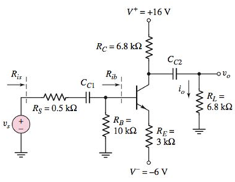
Figure P6.26
(a)
The quiescent
Answer to Problem 6.26P
The quiescent
Explanation of Solution
Given:
The current gain
The circuit for
The circuit parameters are written below.
Concept used:
The expression for quiescent collector current is written below.
Calculation:
Apply dc analysis and KVL in base emitter loop.
Substitute
Substitute
Therefore, the quiescent collector current
Apply KVL in base collector loop.
Substitute
Therefore, the
Conclusion:
Thus, the quiescent
(b)
The hybrid
Answer to Problem 6.26P
The transconductance
Explanation of Solution
Concept used:
The expression for transconductance
The expression for diffusion resistance
The expression for output resistance
Calculation:
Substitute
Therefore, the transconductance
Substitute
Therefore, the diffusion resistance
Substitute
Therefore, the output resistance
Conclusion:
Thus, the transconductance
(c)
The small signal voltage gain
Answer to Problem 6.26P
The small signal voltage gain
Explanation of Solution
Concept used:
The expression for small signal voltage gain
The expression for small signal current gain
Calculation:
The input resistance
Substitute
Therefore, the small signal voltage gain
Substitute
Therefore, the small signal current gain
Conclusion:
Thus, the small signal voltage gain
(d)
The input resistance
Answer to Problem 6.26P
The input resistance
Explanation of Solution
Concept used:
The expression for input resistance
The expression for input resistance
Calculation:
Substitute
Therefore, the input resistance
Substitute
Therefore, the input resistance
Conclusion:
Thus, the input resistance
(e)
The small signal voltage gain
Answer to Problem 6.26P
The small signal voltage gain
Explanation of Solution
Concept used:
The expression for small signal voltage gain
Calculation:
Substitute
Therefore, the small signal voltage gain
Since, small signal current gain is independent of source resistance, so it is same as obtained in part (c).
Therefore, the small signal current gain
Conclusion:
Thus, the small signal voltage gain
Want to see more full solutions like this?
Chapter 6 Solutions
MICROELECT. CIRCUIT ANALYSIS&DESIGN (LL)


- Using an example of your choice, identify the conditions needed for mechanical resonance and measures that can be taken to prevent this from occurring.arrow_forwardCurrent and impedance levels of push-pull RF amplifier. Solid-state RF power amplifiers that provide more than 50 W or so must deal with very large currents, because the typical silicon RF BJT or PET cannot with-stand a DC collector voltage higher than about 40V. (Newer devices using materials such as silicon carbide can exceed this voltage limitation and provide greater power for the same current level.) Suppose a push-pull RF amplifier using a DC collector voltage of 36 V must provide a total peak RF output power of 200W. Typically, the AC "swing" (peak-to-peak AC excursion) of voltage at the collectors cannot exceed twice the DC power-supply voltage. (a) If each of the two devices in the push-pull amplifier delivers IOOW and has a peak-to-peak voltage of (2 x 36) = 72 V across its output terminals , what is the peak current I at the collector of each device, assuming . "d C(PK) smus01 al voltage and current? (b) At this current IC<PK >' how much series inductance L at a…arrow_forwardideally, what should the reactance of a bypass capacitor be in order to eliminate a 10 kHz AC voltage at a given point in an amplifier circuit?arrow_forward
- The parameters for each transistor in the circuit shown in Figure P6.75 areβ = 100 and VA = ∞. (a) Determine the small-signal parameters gm , rπ ,and ro for both transistors. (b) Determine the small-signal voltage gainAv1 = vo1/vs, assuming vo1 is connected to an open circuit, and determinethe gain Av2 = vo/vo1. (c) Determine the overall small-signal voltage gainAv = vo/vs. Compare the overall gain with the product Av1 · Av2, using thevalues calculated in part (b)arrow_forward. Draw and explain the structural overview of MOSFET Capacitances.arrow_forwardConsider the topic LEDs. (a) Explain the working principle of LEDs by using energy band diagram (spontaneous emission), (b) Explain the difference between AMOLEDs and PMOLEDs, (c) Give examples of materials to be used as LEDs with their band gap magnitude. Optoelectronicsarrow_forward
- What is the function of coupling capacitors? Assuming that they are performing their intended function, how do they appear in the ac equivalent circuit? In general, what effect do coupling capacitors have on the gain of an amplifier as a function of frequency?arrow_forwardA single measurement indicates the emitter voltage of the transistor in the circuit of Fig. P6.56 to be 1.0 V. Under the assumption that |VBE| = 0.7 V, what are VB, IB, IE, IC, VC, β, and α ?arrow_forwardCompare hybrid model circuit and re model circuits. Which circuit are you going to recommend in solving AC signal amplifier stage. Defend your answerarrow_forward
 Introductory Circuit Analysis (13th Edition)Electrical EngineeringISBN:9780133923605Author:Robert L. BoylestadPublisher:PEARSON
 Delmar's Standard Textbook Of ElectricityElectrical EngineeringISBN:9781337900348Author:Stephen L. HermanPublisher:Cengage Learning
 Programmable Logic ControllersElectrical EngineeringISBN:9780073373843Author:Frank D. PetruzellaPublisher:McGraw-Hill Education
 Fundamentals of Electric CircuitsElectrical EngineeringISBN:9780078028229Author:Charles K Alexander, Matthew SadikuPublisher:McGraw-Hill Education
 Electric Circuits. (11th Edition)Electrical EngineeringISBN:9780134746968Author:James W. Nilsson, Susan RiedelPublisher:PEARSON
 Engineering ElectromagneticsElectrical EngineeringISBN:9780078028151Author:Hayt, William H. (william Hart), Jr, BUCK, John A.Publisher:Mcgraw-hill Education,