
Concept explainers
Videos
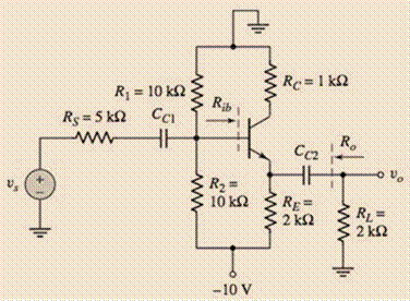
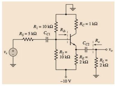
Consider the circuit in Figure P6.45. The transistor parameters are
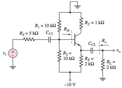
Figure P6.45
a.
The value of the ICQ and VCEQ .
Answer to Problem 6.45P
Explanation of Solution
Given:
The circuit is given as:
Calculation:
Let the BJT be the single node, then by applying Kirchhoff’s current law, the quiescent emitter current
In Common-Emitter mode:
The relation between the quiescent collector current is
For dc analysis,
All the capacitors act as an open circuit and all the ac sources act as short circuits.
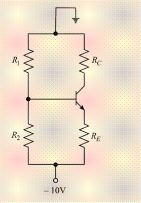
DC analysis:
Redrawing the circuit by open circuit, the capacitors, and short circuit the ac sources.
Evaluating the Thevenin resistance
Evaluating the Thevenin voltage,
Drawing the modified circuit:
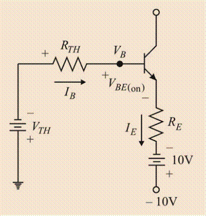
Applying the Kirchhoff s voltage law in the base-emitter loop,
Substituting
From equation (2):
Substituting
Therefore, the value of
From equation (1) and (2):
Substituting
Substitute
Drawing the modified circuit:
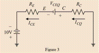
Applying Kirchhoff s voltage law to the loop,
Substituting
Therefore, the value of
b.
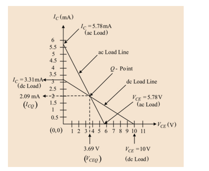
To plot: The dc and the ac load lines.
Explanation of Solution
Given:
The circuit is given as:
Calculation:
Applying Kirchhoff s voltage law around the collector-emitter loop in figure 1.
Substitute
Substitute
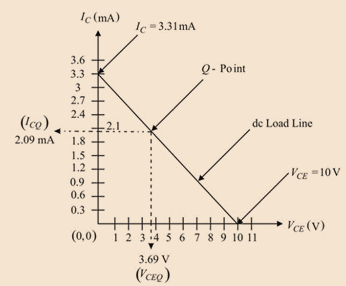
The required “Q” point co-ordinates are
Draw the DC load line:
Drawing the AC equivalent circuit:
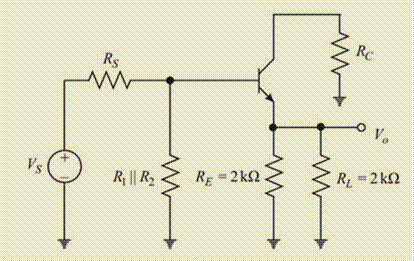
Evaluating the ac load
The expression for the ac load line:
Substitute
Substitute
Drawing the ac load line:
c.
The small signal voltage gain.
Answer to Problem 6.45P
The small signal voltage gain.
Explanation of Solution
Given:
The circuit is given as:
Drawing the small signal analysis of the circuit by short circuiting the dual dc sources and the capacitors:
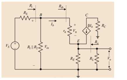
Evaluating the diffusion resistance,
Evaluating the small signal transistor output resistance
Evaluating the input resistance
Calculate the input resistance
The small-signal voltage gain is,
d.
The output resistance.
Answer to Problem 6.45P
The output resistance is
Explanation of Solution
Given:
The circuit is given as
Calculation:
From equation 5,
Thus, the input resistance
Calculate the output resistance,
Therefore, the output resistance
Want to see more full solutions like this?
Chapter 6 Solutions
MICROELECT. CIRCUIT ANALYSIS&DESIGN (LL)


- 6. Through the schematic symbols of MOSFETS, how can you differentiate between a depletion and an enhancement type MOSFET? P-channel or N-channel MOSFET?arrow_forwardDerive an approximate expression for the cavity gain of an SOA in the limiting case of a 3 dB peak–trough ratio.arrow_forwardDiscuss the similarities and differences between sampling & PAM and show the effects of differences on the spectral characteristics of them?arrow_forward
- Describe the combined effect of the RC circuits for higher frequency response in a BJT & FETamplifier. the subject : Analogue Electronics IIarrow_forwardDescribe the state-space representation of a system. How is it different from the transfer function representation, and when is it preferred?arrow_forwardWhat is the transfer function of the circuit?arrow_forward
- Using an example of your choice, identify the conditions needed for mechanical resonance and measures that can be taken to prevent this from occurring.arrow_forwardWhat is the function of coupling capacitors? Assuming that they are performing their intended function, how do they appear in the ac equivalent circuit? In general, what effect do coupling capacitors have on the gain of an amplifier as a function of frequency?arrow_forwardDraw the equivalent Small signal Model and write an equation of Ro .arrow_forward
- ideally, what should the reactance of a bypass capacitor be in order to eliminate a 10 kHz AC voltage at a given point in an amplifier circuit?arrow_forwardSignal designarrow_forwardThe parameters for each transistor in the circuit shown in Figure P6.75 areβ = 100 and VA = ∞. (a) Determine the small-signal parameters gm , rπ ,and ro for both transistors. (b) Determine the small-signal voltage gainAv1 = vo1/vs, assuming vo1 is connected to an open circuit, and determinethe gain Av2 = vo/vo1. (c) Determine the overall small-signal voltage gainAv = vo/vs. Compare the overall gain with the product Av1 · Av2, using thevalues calculated in part (b)arrow_forward
 Introductory Circuit Analysis (13th Edition)Electrical EngineeringISBN:9780133923605Author:Robert L. BoylestadPublisher:PEARSON
 Delmar's Standard Textbook Of ElectricityElectrical EngineeringISBN:9781337900348Author:Stephen L. HermanPublisher:Cengage Learning
 Programmable Logic ControllersElectrical EngineeringISBN:9780073373843Author:Frank D. PetruzellaPublisher:McGraw-Hill Education
 Fundamentals of Electric CircuitsElectrical EngineeringISBN:9780078028229Author:Charles K Alexander, Matthew SadikuPublisher:McGraw-Hill Education
 Electric Circuits. (11th Edition)Electrical EngineeringISBN:9780134746968Author:James W. Nilsson, Susan RiedelPublisher:PEARSON
 Engineering ElectromagneticsElectrical EngineeringISBN:9780078028151Author:Hayt, William H. (william Hart), Jr, BUCK, John A.Publisher:Mcgraw-hill Education,