
Concept explainers
Videos
The parameters of the transistors in the circuit in Figure P10.68 are
The currents
Answer to Problem 10.68P
Explanation of Solution
Given:
Calculation:
The given circuit is,
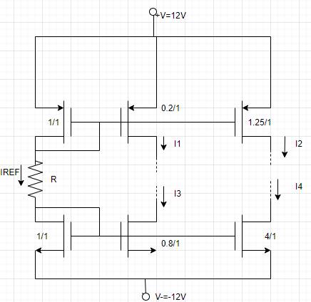
According to the circuit reference current
And
Now substitute the given values in equation (1) and equation (2),
On comparing equation (3) and equation (4),
Now reference current expression is,
Now compare equation (3) and equation (6)
Solve the above expression by quadratic degree method,
Consider
Calculate reference current,
Now calculate current
Conclusion:
Want to see more full solutions like this?
Chapter 10 Solutions
MICROELECT. CIRCUIT ANALYSIS&DESIGN (LL)
Additional Engineering Textbook Solutions
Basic Engineering Circuit Analysis
Introductory Circuit Analysis (13th Edition)
Loose Leaf for Engineering Circuit Analysis Format: Loose-leaf
ELECTRICITY FOR TRADES (LOOSELEAF)
Engineering Electromagnetics
ANALYSIS+DESIGN OF LINEAR CIRCUITS(LL)


- Please answer correctly and as soon as possible. I'll give upvote. Thank you. In the common emitter amplifier given, R1=50Ω, R2=1kΩ and CL=1pF. Determine the quiescent collector current, ICQ, needed such that the unity gain frequency, fu, is equal to 2.4 GHz. Show the complete solution and state all assumptions. The BJT parameters are as follows: β→∞,VA→∞, and Cπ=50 femtofarad (fF). Ignore all other parasitic capacitances and use VT=26mV.arrow_forward2. The output stage of a transmitter requires, owing to supply voltage limitations, a downward impedance transformation of the antenna resistance. The load impedance is 50-Ω. Suppose we wish to deliver 3 Watts of power into such a load at 915 MHz, but the power amplifier has a maximum peak-to-peak sinusoidal voltage of only 7 Volts because of various losses and transistor breakdown problems. Design a two section L-match of low pass type to allow that 3 Watts to be delivered to the 50-Ω load. Assume that all reactive elements are ideal.arrow_forwardFor the circuit shown, let VCC = 3.3 V, RE = 500 Ω, RC = 4 kΩ, R1 = 85 kΩ, R2 = 35 kΩ, and β = 150. Using approximation, determine the Q-point parameters: IBQ, ICQ, and VCEQ. Indicate the exact numerical values, following the given unit.arrow_forward
- When the ltspice simulation of the circuit shown in the figure is performed, the output voltage (Vout) is obtained as given in which of the figures below? NOTE-1: Vcc = 12 V, RC = 2.2 kΩ, RB = 15 kΩ, RE = 180 Ω and C1 = 1 μF. NOTE-2: For the input voltage Vin, the DC offset voltage is 1.6 V, while the applied sinusoidal signal has a amplitude of 10 mV and a frequency of 10 kHz.arrow_forwardSuppose Rc=10 k, Rb=1k, Vcc=4V, Vi =5V, and β= 200. Find Vbe, Vce, Ic, and the region of operation.arrow_forwardIn the common emitter amplifier, R1 = 50Ω, R2 = 1kΩ, and CL=1 pF. Determine the quiescent collector current, ICQ, needed such that the unity gain frequency, fu, = 1 GHz. Show your complete solution and state all your assumptions.arrow_forward
- For a mosfet amplifier circuit, how can I choose an input and output capacitor with poles at 10Hz and 100Hz? Where RC = 1/w.arrow_forward(a) Suppose υbe(t) = 0.005 sin 2000πt V in the bipolar amplifier as shown . Write expressions for υbe(t), vce(t), and υCE(t). (b) What is the maximum value of IC that corresponds to the active region of operation?arrow_forwardIn the circuit in the figure, VGSQ = 6.8 V, IDQ = 2.4 mA, VGS(Th) = 3.3 V, k = 0.4x10⁻³ A/V2, RD = 5.6 kΩ, RF = 2.2 MΩ and rd = 25 kΩ. Accordingly, when a RL = 0.1 kΩ load is connected to the output of the circuit, what will be the voltage gain of the circuit? NOTE: MOSFET output resistance must be taken into account in rd calculationsarrow_forward
- Ex. 1780. A closed-loop system has sustained oscillations (i.e. constant amplitude) with a period of 85 seconds when the gains are: proportional=96, integral=0, and derivative=0. Determine the ideal- PID gains Kp, Ki (minutes^-1), Kd (minutes) using the Ziegler-Nichols method. Also determine the standard-PID values which are commonly used in industry, such as LabVIEW: Kc, Ti (min), Td (min). ans:6arrow_forwardSOLVE NUMBER 2 .1. Solve the output voltage if the gain is 24 db with aninput of 5mV.? 2. Assume a load resistor, RL of 2.2kΩs and a supply voltage of 24v. Calculate the Collector current (Ic) flowing through the load resistor when the transistor is switched fully "ON", assume Vce = 0, & β = 100. Also find the value of the Emitter resistor, Re with a voltage drop of 1.3v across it, R1, R2, and Ib. Assume also a value of 9 times Ib flowing through the resistor R2, while 10 times Ib flowing through R1.arrow_forwardGiven: Voltage Divider Bias Circuit Supply: 10Vdc to 24Vdc Load: 1000 ohms Voltage Gain: 80 to 400 Lower Cutt off Frequency: 100Hz Sinusoidal source (zero internal resistance): 50mVp-p Transistor: Si, beta=75 Base-Collector Capacitance= 8pF Base-Emitter Capacitance= 25pF Design a Single-stage Common Emitter Class A Amplifier and compute the following: a) dc load line b) hie c) midband gain d) Miller equivalent Capacitances e) upper cut off frequencyarrow_forward
 Introductory Circuit Analysis (13th Edition)Electrical EngineeringISBN:9780133923605Author:Robert L. BoylestadPublisher:PEARSON
 Delmar's Standard Textbook Of ElectricityElectrical EngineeringISBN:9781337900348Author:Stephen L. HermanPublisher:Cengage Learning
 Programmable Logic ControllersElectrical EngineeringISBN:9780073373843Author:Frank D. PetruzellaPublisher:McGraw-Hill Education
 Fundamentals of Electric CircuitsElectrical EngineeringISBN:9780078028229Author:Charles K Alexander, Matthew SadikuPublisher:McGraw-Hill Education
 Electric Circuits. (11th Edition)Electrical EngineeringISBN:9780134746968Author:James W. Nilsson, Susan RiedelPublisher:PEARSON
 Engineering ElectromagneticsElectrical EngineeringISBN:9780078028151Author:Hayt, William H. (william Hart), Jr, BUCK, John A.Publisher:Mcgraw-hill Education,