
Videos
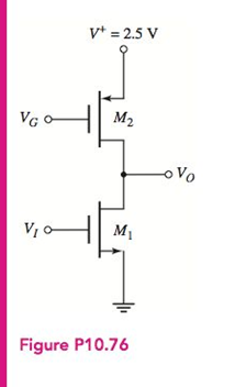
For the circuit shown in Figure P10.76, the transistor parameters are
(a)
The
Answer to Problem 10.76P
Explanation of Solution
Given:
Calculation:
The given circuit is,

The small-signal voltage gain is given, the expression for gain is,
Substituting the given values,
Substitute
Now substitute the given values in above expression,
It is known that,
On putting the given values,
Now substitute the value of
The drain current
Hence
Substitute
Put the value of
Conclusion:
(b)
The voltage
Answer to Problem 10.76P
Explanation of Solution
Given:
Calculation:
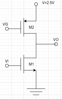
The given circuit is,

The small-signal voltage gain is given, the expression for gain is,
Substituting the given values,
Substitute
Now substitute the given values in above expression,
It is known that,
On putting the given values,
Now substitute the value of
The drain current
Hence
Substitute
Put the value of
Substitute
Conclusion:
(c)
The voltage
Answer to Problem 10.76P
Explanation of Solution
Given:
Calculation:
The given circuit is,
The small-signal voltage gain is given, the expression for gain is,
Substituting the given values,
Substitute
Now substitute the given values in above expression,
It is known that,
On putting the given values,
Now substitute the value of
The drain current
Hence
Substitute
Put the value of
Since
The drain current
On substituting the given values,
Now the gate voltage will be,
Conclusion:
Want to see more full solutions like this?
Chapter 10 Solutions
MICROELECT. CIRCUIT ANALYSIS&DESIGN (LL)


- In the circuit given in the figure, what is the voltage gain (Av) of the circuit when = 100, r0 = 40 kΩ, RB = 360 kΩ, RC = 3.3 kΩ, RE = 220 Ω, Rs = 15 kΩ and RL = 166 kΩ?NOTE-1: The output impedance r0 of the transistor will be taken into the calculations.NOTE-2: Capacitors are negligible at mid-band frequency.arrow_forwardIn the common emitter amplifier, R1 = 50Ω, R2 = 1kΩ, and CL=1 pF. Determine the quiescent collector current, ICQ, needed such that the unity gain frequency, fu, = 1 GHz. Show your complete solution and state all your assumptions.arrow_forwardFor each transistor shown in Figure P10.1,determine whether the BE and BC junctions areforward- or reverse-biased, and determine theoperating region.arrow_forward
- The following parameters of NMOS used in the circuit in the figure are given. Al = NA K „= 100µA / V² 0 = Y C = 25 fF C, = 100 fF Accordingly; a) What is the cutoff frequency of the circuit? b) What is the upper cutoff frequency of the circuit?arrow_forwardDraw, Illustrate and label your schematic diagram before solving the problem. 1) Given a Fixed-Biased transistor circuit with Beta DC is 200 , voltage at common collector is +22v ,base supply voltage is +11V, Base resistor is 47kOhms , collector resistor is 390 ohms ,Voltage at Base-emitter junction is 0.7v. Determine the Q-point of collector current and Voltage at collector-emitter junction. These might be help as a guide to solve the problem.arrow_forwardDetermine the folowing A.base current (IB), B. collector current (Ic), C. collector-to-emitter voltage (VCE),D. draw the load line, locate the Q-pointF. input impedance (Zi),G. Output impedance (Zo)arrow_forward
- a) Differentiate between Common Emitter (CE), Common Collector (CC) and Common Base (CB) amplifiers. b) Do the DC Analysis of the circuit below and find out the DC collector voltage?c) Do the AC Analysis of the circuit below and find out the AC collector voltage?R1=30kΩΩ=610Ωarrow_forward1) Find the operating point of the transistor by drawing the load line of the BJT transistor circuit given below. Calculate the voltage values VE and VC. (β = 100, VBE = 0.7 V, R1 = 10 KΩ, RC = 4.7 KΩ, RE = 3.3 KΩ, VCC = 10 V, VEE = - 4 V)arrow_forwardA MOSFET common-source amplifier must amplify a sinusoidal ac signal with a peak amplitude of 0.4 V. What is the minimum value of VGS −VT Nfor the transistor? If a voltage gain of 26 dB is required, what is the minimum power supply voltage?arrow_forward
- Describe the combined effect of the RC circuits for higher frequency response in a BJT & FETamplifier. the subject : Analogue Electronics IIarrow_forwardConsider the common-source amplifier shown in Figure P11.50. The NMOS transistor has KP=50 μA/V2, L=5 μm, W=500 μm, Vto=1 V and rd=∞.a. Determine the values of IDQ, VDSQ and gm. b. Compute the voltage gain, input resistance, and output resistance, assuming that the coupling capacitors are short circuits for the ac signal. Repeat Problem P11.50 for an NMOS transistor having KP=50 μA/V2, W=600 μm, L=20 μm, Vto=2 V and rd=∞. Compare the gain with that attained in Problem P11.50.arrow_forwardIn the circuit in the figure, VGSQ = 6.8 V, IDQ = 2.4 mA, VGS(Th) = 3.3 V, k = 0.4x10⁻³ A/V2, RD = 5.6 kΩ, RF = 2.2 MΩ and rd = 25 kΩ. Accordingly, when a RL = 0.1 kΩ load is connected to the output of the circuit, what will be the voltage gain of the circuit? NOTE: MOSFET output resistance must be taken into account in rd calculationsarrow_forward
 Introductory Circuit Analysis (13th Edition)Electrical EngineeringISBN:9780133923605Author:Robert L. BoylestadPublisher:PEARSON
 Delmar's Standard Textbook Of ElectricityElectrical EngineeringISBN:9781337900348Author:Stephen L. HermanPublisher:Cengage Learning
 Programmable Logic ControllersElectrical EngineeringISBN:9780073373843Author:Frank D. PetruzellaPublisher:McGraw-Hill Education
 Fundamentals of Electric CircuitsElectrical EngineeringISBN:9780078028229Author:Charles K Alexander, Matthew SadikuPublisher:McGraw-Hill Education
 Electric Circuits. (11th Edition)Electrical EngineeringISBN:9780134746968Author:James W. Nilsson, Susan RiedelPublisher:PEARSON
 Engineering ElectromagneticsElectrical EngineeringISBN:9780078028151Author:Hayt, William H. (william Hart), Jr, BUCK, John A.Publisher:Mcgraw-hill Education,