Microelectronics Circuit Analysis and Design
4th Edition
ISBN: 9780077387815
Author: NEAMEN
Publisher: DGTL BNCOM
bartleby

Videos

Question
Book Icon
Chapter 16, Problem 16.62P

(a)

To determine

To construct: The table for the state of each transistor.

To find: The output voltage vO1 , vO2 and vO3 for the input logic state.

(a)

Expert Solution
Check Mark

Answer to Problem 16.62P

The value of the output voltages is obtained and is shown in Table 2

Explanation of Solution

Calculation:

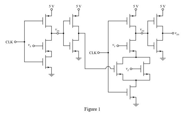
The given diagram is shown in Figure 1

  Microelectronics Circuit Analysis and Design, Chapter 16, Problem 16.62P

The given table is shown in Table 1

Table 1

    StateCLKvXvYvZ
    10000
    21111
    30000
    41011
    50000
    61101

For state 1

The input clock signal input X, Y and Z are at logic zero and the logic function of the output voltage vO1 is the compliment of the input voltage vX an is given by,

  vO1=v¯X   ....... (1).

Substitute 0 for vX in the above equation.

  vO1=0¯=1

From the circuit the NMOS device with the input vY is in series with the parallel combination of the NMOS device of input vZ and the compliment vo1 .

The expression for the logic function of the output voltage vo2 is given by,

  vO2=vY( v ¯ O1+vZ)¯   ...... (2)

Substitute 1 for vO1 , 0 for vY and 0 for vZ in the above equation.

  vO2=0( 1 ¯ +0)¯=1

The logic function of the output voltage vO3 is the compliment of the output voltage vO2 and is given by,

  vO3=vO2¯   ...... (3)

Substitute 1 for vO2 in the above equation.

  vO3=1¯=0

For state 2.

All the inputs are at logic 1.

Substitute 1 for vX in equation (1)

  vO1=1¯=0

Substitute 0 for vO1 , 1 for vY and 1 for vZ in equation (2)

  vO2=1( 0 ¯ +1)¯=1

Substitute 0 for vO2 in equation (3)

  vO3=0¯=1

For state 3.

All the inputs are at logic 0.

Substitute 0 for vX in equation (1)

  vO1=0¯=1

Substitute 1 for vO1 , 0 for vY and 0 for vZ in equation (2)

  vO2=0( 1 ¯ +0)¯=1

Substitute 1 for vO2 in equation (3)

  vO3=1¯=0

For state 4.

The input clock, vY and the input vZ are at logic zero and the input vX is at logic zero.

Substitute 0 for vX in equation (1)

  vO1=0¯=1

Substitute 1 for vO1 , 1 for vY and 1 for vZ in equation (2)

  vO2=1( 1 ¯ +1)¯=0

Substitute 0 for vO2 in equation (3)

  vO3=0¯=1

For state 5.

All the inputs are at logic zero.

Substitute 0 for vX in equation (1)

  vO1=0¯=1

Substitute 1 for vO1 , 0 for vY and 0 for vZ in equation (2)

  vO2=0( 1 ¯ +0)¯=1

Substitute 1 for vO2 in equation (3)

  vO3=1¯=0

For state 6.

The input clock, vX and the input vZ are at logic zero and the input vY is at logic zero.

Substitute 1 for vX in equation (1)

  vO1=1¯=0

Substitute 0 for vO1 , 0 for vY and 1 for vZ in equation (2)

  vO2=0( 0 ¯ +1)¯=1

Substitute 1 for vO2 in equation (3)

  vO3=1¯=0

The table for the state of the transistors and the output voltage is shown in table below.

The required table is shown in Table 2

Table 2

    StateCLKvXvYvZvO1vO2vO3
    100005V5V0V
    211110V0V5V
    300005V5V0V
    410115V5V
    500005V5V0V
    611010V5V0V

The table for the state of the transistor is shown below.

Conclusion:

Therefore, the value of the output voltages is obtained and is shown in Table 2

(b)

To determine

The logic function that the circuit implements.

(b)

Expert Solution
Check Mark

Answer to Problem 16.62P

The logic that the circuit performs is (vXORvZ)ANDvY .

Explanation of Solution

Calculation:

The expression for the output voltage vO3 is given by,

  vO3=v¯O3

Substitute vY( v ¯ O1+vZ)¯ for vO2 in the above equation.

  vO3= v Y ( v ¯ O1 + v Z )¯¯=(vX+vZ)vY=(vXORvZ)ANDvY

Conclusion:

Therefore, the logic that the circuit performs is (vXORvZ)ANDvY .

Want to see more full solutions like this?

Subscribe now to access step-by-step solutions to millions of textbook problems written by subject matter experts!
Students have asked these similar questions
Sketch the VTC for a logic inverter with VoH = 5 V, Vol = 0.2 V, V.IL= 1.4 V, and VIH= 1.6 V. Also, determine the logic swing , transition width, and the noise margins.
RD* = 1 for a memory read bus operation.  True  False
Consider single phase full bridge SPWM inverter with switching frequency 1050 Hz, amplitude modulationratio vcontrol/vtriangle ma is 0.8, frequency modulation ratio mf is 21, input voltage Vin= 400VDC calculate efectivevalue and frequency of the output voltage fundamental frequency component

Chapter 16 Solutions

Microelectronics Circuit Analysis and Design

Ch. 16 - Consider the NMOS logic circuit in Figure 16.18....Ch. 16 - Repeat Exercise TYU 16.5 for the NMOS logic...Ch. 16 - The CMOS inverter in Figure 16.21 is biased at...Ch. 16 - swA CMOS inverter is biased at VDD=3V . The...Ch. 16 - A CMOS inverter is biased at VDD=1.8V . The...Ch. 16 - Prob. 16.7TYUCh. 16 - Repeat Exercise Ex 16.9 for a CMOS inverter biased...Ch. 16 - Determine the transistor sizes of a 3input CMOS...Ch. 16 - Design the widthtolength ratios of the transistors...Ch. 16 - Design a static CMOS logic circuit that implements...Ch. 16 - Prob. 16.10TYUCh. 16 - Prob. 16.11TYUCh. 16 - Sketch a clocked CMOS logic circuit that realizes...Ch. 16 - Prob. 16.12EPCh. 16 - Prob. 16.13TYUCh. 16 - Consider the CMOS transmission gate in Figure...Ch. 16 - Prob. 16.15TYUCh. 16 - Prob. 16.14EPCh. 16 - Prob. 16.16TYUCh. 16 - Prob. 16.17TYUCh. 16 - Sketch the quasistatic voltage transfer...Ch. 16 - Sketch an NMOS threeinput NOR logic gate. Describe...Ch. 16 - Discuss how more sophisticated (compared to the...Ch. 16 - Sketch the quasistatic voltage transfer...Ch. 16 - Discuss the parameters that affect the switching...Ch. 16 - Prob. 6RQCh. 16 - Sketch a CMOS threeinput NAND logic gate. Describe...Ch. 16 - sDiscuss how more sophisticated (compared to the...Ch. 16 - Prob. 9RQCh. 16 - Sketch an NMOS transmission gate and describe its...Ch. 16 - Sketch a CMOS transmission gate and describe its...Ch. 16 - Discuss what is meant by pass transistor logic.Ch. 16 - Prob. 13RQCh. 16 - Prob. 14RQCh. 16 - Prob. 15RQCh. 16 - Describe the basic architecture of a semiconductor...Ch. 16 - ‘Sketch a CMOS SRAM cell and describe its...Ch. 16 - Prob. 18RQCh. 16 - Describe a maskprogrammed MOSFET ROM memory.Ch. 16 - Describe the basic operation of a floating gate...Ch. 16 - Prob. 16.1PCh. 16 - Prob. 16.2PCh. 16 - (a) Redesign the resistive load inverter in Figure...Ch. 16 - Prob. D16.4PCh. 16 - Prob. 16.5PCh. 16 - Prob. D16.6PCh. 16 - Prob. 16.7PCh. 16 - Prob. 16.8PCh. 16 - For the depletion load inverter shown in Figure...Ch. 16 - Prob. 16.10PCh. 16 - Prob. D16.11PCh. 16 - Prob. D16.12PCh. 16 - Prob. 16.13PCh. 16 - For the two inverters in Figure P16.14, assume...Ch. 16 - Prob. 16.15PCh. 16 - Prob. 16.16PCh. 16 - Prob. 16.17PCh. 16 - Prob. 16.18PCh. 16 - Prob. D16.19PCh. 16 - Prob. 16.20PCh. 16 - Prob. 16.21PCh. 16 - Prob. 16.22PCh. 16 - In the NMOS circuit in Figure P16.23, the...Ch. 16 - Prob. 16.24PCh. 16 - Prob. 16.25PCh. 16 - Prob. 16.26PCh. 16 - What is the logic function implemented by the...Ch. 16 - Prob. D16.28PCh. 16 - Prob. D16.29PCh. 16 - Prob. 16.31PCh. 16 - Prob. 16.32PCh. 16 - Prob. 16.33PCh. 16 - Consider the CMOS inverter pair in Figure P16.34....Ch. 16 - Prob. 16.35PCh. 16 - Prob. 16.36PCh. 16 - Prob. 16.37PCh. 16 - Prob. 16.38PCh. 16 - Prob. 16.39PCh. 16 - (a) A CMOS digital logic circuit contains the...Ch. 16 - Prob. 16.41PCh. 16 - Prob. 16.42PCh. 16 - Prob. 16.43PCh. 16 - Prob. 16.44PCh. 16 - Prob. 16.45PCh. 16 - Prob. 16.46PCh. 16 - Prob. 16.47PCh. 16 - Prob. 16.48PCh. 16 - Prob. 16.49PCh. 16 - Prob. 16.50PCh. 16 - Prob. 16.51PCh. 16 - Prob. 16.52PCh. 16 - Prob. D16.53PCh. 16 - Figure P16.54 is a classic CMOS logic gate. (a)...Ch. 16 - Figure P16.55 is a classic CMOS logic gate. (a)...Ch. 16 - Consider the classic CMOS logic circuit in Figure...Ch. 16 - (a) Given inputs A,B,C,A,B and C , design a CMOS...Ch. 16 - (a) Given inputs A, B, C, D, and E, design a CMOS...Ch. 16 - (a) Determine the logic function performed by the...Ch. 16 - Prob. D16.60PCh. 16 - Prob. 16.61PCh. 16 - Prob. 16.62PCh. 16 - Sketch a clocked CMOS domino logic circuit that...Ch. 16 - Sketch a clocked CMOS domino logic circuit that...Ch. 16 - Prob. D16.65PCh. 16 - Prob. 16.66PCh. 16 - Prob. 16.67PCh. 16 - The NMOS transistors in the circuit shown in...Ch. 16 - Prob. 16.69PCh. 16 - Prob. 16.70PCh. 16 - Prob. 16.71PCh. 16 - (a) Design an NMOS pass transistor logic circuit...Ch. 16 - Prob. 16.73PCh. 16 - What is the logic function implemented by the...Ch. 16 - Prob. 16.75PCh. 16 - Prob. 16.76PCh. 16 - Prob. 16.77PCh. 16 - Consider the NMOS RS flipflop in Figure 16.63...Ch. 16 - Prob. 16.79PCh. 16 - Consider the circuit in Figure P16.80. Determine...Ch. 16 - Prob. D16.81PCh. 16 - Prob. 16.82PCh. 16 - Prob. 16.83PCh. 16 - Prob. 16.84PCh. 16 - (a) A 1 megabit memory is organized in a square...Ch. 16 - Prob. 16.86PCh. 16 - Prob. 16.87PCh. 16 - Prob. 16.88PCh. 16 - Prob. D16.89PCh. 16 - Prob. 16.90PCh. 16 - Prob. 16.91PCh. 16 - Prob. 16.92PCh. 16 - Prob. D16.93PCh. 16 - Prob. D16.94PCh. 16 - Prob. D16.95PCh. 16 - An analog signal in the range 0 to 5 V is to be...Ch. 16 - Prob. 16.97PCh. 16 - Prob. 16.98PCh. 16 - Prob. 16.99PCh. 16 - The weightedresistor D/A converter in Figure 16.90...Ch. 16 - The Nbit D/A converter with an R2R ladder network...Ch. 16 - Prob. 16.102PCh. 16 - Prob. 16.103PCh. 16 - Prob. 16.104PCh. 16 - Prob. 16.105PCh. 16 - Design a classic CMOS logic circuit that will...Ch. 16 - Prob. D16.111DPCh. 16 - Prob. D16.112DPCh. 16 - Prob. D16.113DP
Knowledge Booster
Background pattern image
Electrical Engineering
Learn more about
Need a deep-dive on the concept behind this application? Look no further. Learn more about this topic, electrical-engineering and related others by exploring similar questions and additional content below.
Similar questions
SEE MORE QUESTIONS
Recommended textbooks for you
Text book image
Introductory Circuit Analysis (13th Edition)
Electrical Engineering
ISBN:9780133923605
Author:Robert L. Boylestad
Publisher:PEARSON
Text book image
Delmar's Standard Textbook Of Electricity
Electrical Engineering
ISBN:9781337900348
Author:Stephen L. Herman
Publisher:Cengage Learning
Text book image
Programmable Logic Controllers
Electrical Engineering
ISBN:9780073373843
Author:Frank D. Petruzella
Publisher:McGraw-Hill Education
Text book image
Fundamentals of Electric Circuits
Electrical Engineering
ISBN:9780078028229
Author:Charles K Alexander, Matthew Sadiku
Publisher:McGraw-Hill Education
Text book image
Electric Circuits. (11th Edition)
Electrical Engineering
ISBN:9780134746968
Author:James W. Nilsson, Susan Riedel
Publisher:PEARSON
Text book image
Engineering Electromagnetics
Electrical Engineering
ISBN:9780078028151
Author:Hayt, William H. (william Hart), Jr, BUCK, John A.
Publisher:Mcgraw-hill Education,
CMOS Tech: NMOS and PMOS Transistors in CMOS Inverter (3-D View); Author: G Chang;https://www.youtube.com/watch?v=oSrUsM0hoPs;License: Standard Youtube License