
Concept explainers
Videos
Consider the NMOS inverter with resistor load in Figure 16.3(a) biased at
(a)
The value of
Answer to Problem 16.1EP
The value of
Explanation of Solution
Given:
Calculation:
Consider the NMOS inverter with resister load biased at
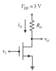
Figure 1
From the circuit,
Calculate the value of
Since,
The current drain equation is,
Apply Kirchhoff’s voltage law to the circuit.
Conclusion:
Therefore, the value of
(b)
The maximum current and maximum power dissipation in the inverter.
Answer to Problem 16.1EP
The maximum power transfer is,
The maximum drain current is,
Explanation of Solution
Given:
Calculation:
Consider Figure 1.
The maximum current is,
The maximum power transfer is,
Conclusion:
Therefore, the maximum power transfer is,
(c)
The transition point for the driver transistor.
Answer to Problem 16.1EP
The transition point for the driver transistor is
Explanation of Solution
Given:
Calculation:
Transitionpoints for the driver resistor is
As the transition voltage is positive and greater than zero for NMOS, the input transition voltage is
The output transition voltage is,
Conclusion:
Therefore, the transition point are
Want to see more full solutions like this?
Chapter 16 Solutions
Microelectronics Circuit Analysis and Design


- Wire delay I. Calculate the delay of a 10 mm wire in 28 nm technology that is divided into 20 0.5 mm segments with a 20× minimum-size inverter driving each segment.arrow_forwardA two-stage inverter is shown in this figure. Vs=50 V. v=110V2 sin 100 nt. The average voltage of C is set to be 200 V.1=2 A. The bipolar modulation scheme is applied on the inverter and the power factor of the inverter is set to be 1. Consider the two-stage inverter is lossless, Calculate the current of L. il (ii) Assume the voltage of Cr is a constant DC voltage of 200 V. Calculate the instantaneous duty ratio of the inverter. din if C = 75 HF, calculate the highest and lowest voltage of Cr.arrow_forwardDesign an asymmetrical inverter to meet the delay of 250 ps for a load capacitance of 120 fF. Use VDD =1.5V, VTN =0.50 V, and VTP =−0.50 V. with (W/L)P = (W/L)N .arrow_forward
- A high-performance microprocessor design requires 200 million logic gates and is placed in apackage that can dissipate 100 W. (a) What is theaverage power that can be dissipated by each logicgate on the chip? (b) If a supply voltage of 1.8 V isused, how much current can be used by each gate?Assume a 33 percent duty cycle. (c) If the averagegate delay for these circuits must be 1 ns, what isthe power-delay product required for the circuits inthis design?arrow_forwardImplement F(A,B,C)= m2+m5+m6+m7, using the smallest possible multiplexer and inverters as needed.arrow_forwardDesign an asymmetrical inverter to meet the delay specification a symmetrical CMOS reference inverter to provide a propagation delay of 400 ps fora load capacitance of 200 fF. Use VDD =2.5 V, VTN =0.60 V, and VTP =−0.60 V.with (W/L)P = (W/L)N .arrow_forward
- What is the power-delay product for a symmetrical CMOSinverter with (W/L)N = 2/1, (W/L)P = 5/1,VDD = 2.5 V, and C = 0.3 pF? (b) Repeat forVDD = 2.0 V. (c) Repeat for VDD = 1.8 V.? How much power does the inverter dissipate if it is switching at a frequency of 100 MHz?arrow_forwardAssume the following values for the inverter circuit parameters: Vs = 6v, VT = 0.9v RL = 5kΩ, k’nVOV = 0.25 Determine a (W/L) sizing for the MOSFET so that the inverter gate output for a logical 0 is able to switch OFF the MOSFET of another inverter.arrow_forwardCalculate the storage time for the inverter as shown if IBF = 2.5 mA, IBR = −0.5 mA,τF = 0.4 ns, and τR = 12 ns. Use Table shown.arrow_forward
- Consider two microprocessors having 8-bit and 16-bit wide external data buses, respectfully. The two processors are identical otherwise and their bus cycles are the same speed. Suppose all instructions and operands are two Bytes. By what factor do the maximum data transfer rates vary? Suppose all instructions and operands are one Byte. By what factor do the maximum data transfer rates vary? Discuss your answers.arrow_forwardDesign an NMOS depletion load inverter (VDD =3.3 V, VL = 0.20 V, VTNS = 0.75 V, VTNL = −2 V,γ = 0) to have an average propagation delay of 1 nswith a capacitive load of 0.2 pF. What is the averagestatic power dissipation of this gate?arrow_forward1. A square-wave inverter has an R-L load with R=15 Ω and L=10 mH. The inverter output frequency is400 Hz (fundamental frequency).(a) Determine the values of the required to establish a load current which has a fundamentalfrequency component of 10 A rms with α = 0.(b) For a controlled full-bridge inverter, the dc source is 125 V and the switching frequency is60 Hz. Determine the value of α to produce an output with amplitude of 100 V at the fundamentalfrequency.arrow_forward
 Introductory Circuit Analysis (13th Edition)Electrical EngineeringISBN:9780133923605Author:Robert L. BoylestadPublisher:PEARSON
 Delmar's Standard Textbook Of ElectricityElectrical EngineeringISBN:9781337900348Author:Stephen L. HermanPublisher:Cengage Learning
 Programmable Logic ControllersElectrical EngineeringISBN:9780073373843Author:Frank D. PetruzellaPublisher:McGraw-Hill Education
 Fundamentals of Electric CircuitsElectrical EngineeringISBN:9780078028229Author:Charles K Alexander, Matthew SadikuPublisher:McGraw-Hill Education
 Electric Circuits. (11th Edition)Electrical EngineeringISBN:9780134746968Author:James W. Nilsson, Susan RiedelPublisher:PEARSON
 Engineering ElectromagneticsElectrical EngineeringISBN:9780078028151Author:Hayt, William H. (william Hart), Jr, BUCK, John A.Publisher:Mcgraw-hill Education,