
Concept explainers
Videos
(a)
The value of the voltage
(a)
Answer to Problem 16.8P
The maximum value of the voltage
Explanation of Solution
Calculation:
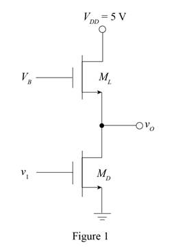
The given diagram is shown in Figure 1.
The expression for the voltage
Substitute
The expression for the enhancement mode NMOS inverter equation is given by,
Substitute
Conclusion:
Therefore, the maximum value of the voltage
(b)
The value of the voltage
(b)
Answer to Problem 16.8P
The maximum value of the voltage
Explanation of Solution
Calculation:
The expression for the voltage
Substitute
Consider the input voltage
The expression for the enhancement mode NMOS inverter equation is given by,
Substitute
Conclusion:
Therefore, the maximum value of the voltage
(c)
The value of the voltage
(c)
Answer to Problem 16.8P
The maximum value of the voltage
Explanation of Solution
Calculation:
The expression for the voltage
Substitute
Consider the input voltage
The expression for the enhancement mode NMOS inverter equation is given by,
Substitute
Conclusion:
Therefore, the maximum value of the voltage
(d)
The value of the voltage
(d)
Answer to Problem 16.8P
The maximum value of the voltage
Explanation of Solution
Calculation:
The expression for the voltage
Substitute
Consider the input voltage
The expression for the enhancement mode NMOS inverter equation is given by,
Substitute
Conclusion:
Therefore, the maximum value of the voltage
Want to see more full solutions like this?
Chapter 16 Solutions
MICROELECT. CIRCUIT ANALYSIS&DESIGN (LL)


- (a) What is the power-delay product for a symmetrical CMOS inverterwith (W/L)N =2/1, (W/L)P =5/1, C =0.25 pF,VDD =3.3 V, VTN =0.75 V, and VTP =−0.75 V? (b) Estimate the maximum switchingfrequency for this inverter. (c) Howmuch powerdoes the inverter dissipate if it is switching at thefrequency found in (b)?arrow_forwardGiven Vdd=3.3V, Kn=100uA/V2 , Kp=20uA/V2,Vtn = 0.6V, and Vtp = -0.6V. Determine the Voltage Transfer Characteristics points indicated by the pseudo-NMOS inverter circuit.arrow_forwardA CMOS inverter has (W/L)N =2/1,(W/L)P =5/1 for VDD = 2.0 V, VTN =0.45 V, and VTP = −0.55 V. for VDD = 2.0 V, VTN = 0.55 V,and VTP = −0.45 V.What is the peak current in the logicgate and at what input voltage does it occur?arrow_forward
- What are the noise margins of a minimum size CMOS inverter in which both W/L ratios are 2/1 and VDD = 2.5 V and VTN = −VTP = 0.6 V?arrow_forwardDesign an asymmetrical inverter to meet the delay specificationa symmetrical CMOS reference inverter to provide a delay of 1 ns when driving a 10-pF load.(a) Assume VDD =2.5 V. (b) Assume VDD =1.8 V and VT N =−VT P =0.45 V. with (W/L)P = 2(W/L)N .arrow_forwardIf,for a single phase half bridge inverter the amplitude of output voltage is Vs and the output power is P then their corresponding values for a single phase full-bridge inverter are a. 2Vs,2P b. 2Vs,4P c. 2Vs,P d. Vs,Parrow_forward
- Design an asymmetrical inverter to meet the delay specification a symmetrical CMOS reference inverter to provide a propagation delay of 400 ps fora load capacitance of 200 fF. Use VDD =2.5 V, VTN =0.60 V, and VTP =−0.60 V.with (W/L)P = (W/L)N .arrow_forwardSketch the VTC for a logic inverter with VoH = 5 V, Vol = 0.2 V, V.IL= 1.4 V, and VIH= 1.6 V. Also, determine the logic swing , transition width, and the noise margins.arrow_forwardDesign an NMOS depletion load inverter (VDD =3.3 V, VL = 0.20 V, VTNS = 0.75 V, VTNL = −2 V,γ = 0) to have an average propagation delay of 1 nswith a capacitive load of 0.2 pF. What is the averagestatic power dissipation of this gate?arrow_forward
- Prove mathematically that if ??/??= 1 in an inverter, the inverter threshold voltage (input voltage at thepoint of sharp transition) = VDD/2. Determine the inverter threshold voltage if ??/??=1/5and Vt=100mV.arrow_forward1. A square-wave inverter has an R-L load with R=15 Ω and L=10 mH. The inverter output frequency is400 Hz (fundamental frequency).(a) Determine the values of the required to establish a load current which has a fundamentalfrequency component of 10 A rms with α = 0.(b) For a controlled full-bridge inverter, the dc source is 125 V and the switching frequency is60 Hz. Determine the value of α to produce an output with amplitude of 100 V at the fundamentalfrequency.arrow_forwardDescribe the C-V characteristics of a MOS capacitor and explain the physics behind them. 2. Draw the IV curve of a MOSFET for different gate voltages. Explain the characteristics of the curve and dependence on the gate voltage. 3. Explain the structure and operation principle of a CMOS inverter. What are its benefits? 4. Compare SRAM, DRAM and Flash memoriesarrow_forward
 Introductory Circuit Analysis (13th Edition)Electrical EngineeringISBN:9780133923605Author:Robert L. BoylestadPublisher:PEARSON
 Delmar's Standard Textbook Of ElectricityElectrical EngineeringISBN:9781337900348Author:Stephen L. HermanPublisher:Cengage Learning
 Programmable Logic ControllersElectrical EngineeringISBN:9780073373843Author:Frank D. PetruzellaPublisher:McGraw-Hill Education
 Fundamentals of Electric CircuitsElectrical EngineeringISBN:9780078028229Author:Charles K Alexander, Matthew SadikuPublisher:McGraw-Hill Education
 Electric Circuits. (11th Edition)Electrical EngineeringISBN:9780134746968Author:James W. Nilsson, Susan RiedelPublisher:PEARSON
 Engineering ElectromagneticsElectrical EngineeringISBN:9780078028151Author:Hayt, William H. (william Hart), Jr, BUCK, John A.Publisher:Mcgraw-hill Education,