
Concept explainers
Videos
(a)
The design parameter for the circuit.
(a)
Answer to Problem D16.11P
The required value of the width to length ratio of the driver is
Explanation of Solution
Calculation:
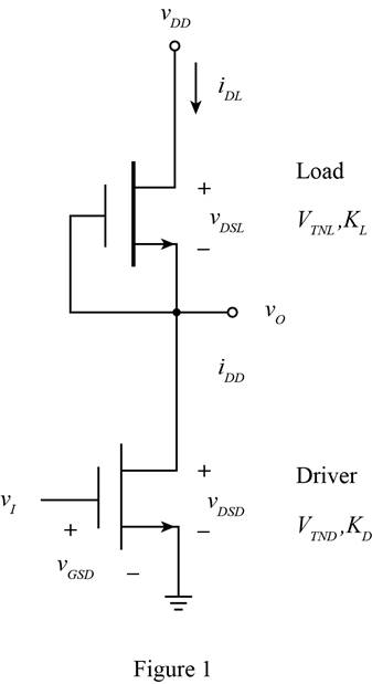
The given diagram is shown in Figure 1
The expression to determine the power dissipated in the circuit is given by,
Substitute
The expression to determine the value of the drain current is given by,
Substitute
The expression to determine the value of the width to length ratio of the driver and the load transistor is given by,
Substitute
The expression for the ratio of the width to length ratio of driver to transistor is given by,
Substitute
Conclusion:
Therefore, the required value of the width to length ratio of the driver is
(b)
The transition for the driver and the load transistor.
(b)
Answer to Problem D16.11P
The value of the input transition point or the load is
Explanation of Solution
Calculation:
For load.
The expression to determine the value of the output transition point is given by,
Substitute
The expression to determine the input transition point is given by,
Substitute
For driver.
The expression to determine the input transition point is given by,
Substitute
The expression to determine the value of the output transition point is given by,
Substitute
Conclusion:
Therefore, the value of the input transition point or the load is
(c)
The value of maximum power dissipation in the inverter and the output voltage for the given input.
(c)
Answer to Problem D16.11P
The value of the output voltage is
Explanation of Solution
Calculation:
The power dissipation is same even if the width to length ratio of the driver is doubled and is given by,
The expression to determine the value of the drain current is given by,
Substitute
The expression for the width to length ratio of the driver is given by,
Substitute
The expression for the ratio of the width to length ratio of driver to transistor is given by,
Substitute
The expression to determine the value of the output voltage is given by,
Substitute
Conclusion:
Therefore, the value of the output voltage is
Want to see more full solutions like this?
Chapter 16 Solutions
MICROELECT. CIRCUIT ANALYSIS&DESIGN (LL)


- 1. Draw the transistor level Diagram for the expression Y = (A+B) C+CD using CMOS technology. Also sketch the stick diagram. 2. Describe the read and write operation of a 6T SRAM cell with necessary figures.arrow_forwardDesign an asymmetrical inverter to meet the delay specification a symmetrical CMOS reference inverter to provide a propagation delay of 400 ps fora load capacitance of 200 fF. Use VDD =2.5 V, VTN =0.60 V, and VTP =−0.60 V.with (W/L)P = (W/L)N .arrow_forwardImplement F(A,B,C)= m2+m5+m6+m7, using the smallest possible multiplexer and inverters as needed.arrow_forward
- Given Vdd=3.3V, Kn=100uA/V2 , Kp=20uA/V2,Vtn = 0.6V, and Vtp = -0.6V. Determine the Voltage Transfer Characteristics points indicated by the pseudo-NMOS inverter circuit.arrow_forward1. A square-wave inverter has an R-L load with R=15 Ω and L=10 mH. The inverter output frequency is400 Hz (fundamental frequency).(a) Determine the values of the required to establish a load current which has a fundamentalfrequency component of 10 A rms with α = 0.(b) For a controlled full-bridge inverter, the dc source is 125 V and the switching frequency is60 Hz. Determine the value of α to produce an output with amplitude of 100 V at the fundamentalfrequency.arrow_forwardWhat are the rise time, fall time, and average propagation delay for a symmetrical CMOS inverter with (W/L)N =2/1, (W/L)P =5/1, C =0.25 pF, VDD =3.3 V, VTN =0.75 V, and VTP =−0.75 V?arrow_forward
- A high-performance microprocessor design requires 200 million logic gates and is placed in apackage that can dissipate 100 W. (a) What is theaverage power that can be dissipated by each logicgate on the chip? (b) If a supply voltage of 1.8 V isused, how much current can be used by each gate?Assume a 33 percent duty cycle. (c) If the averagegate delay for these circuits must be 1 ns, what isthe power-delay product required for the circuits inthis design?arrow_forward(a) A CMOS inverter has (W/L)N =2/1,(W/L)P =5/1, and VDD =3.3 V. Assume VTN =−VTP =0.8 V. What is the peak current in the logicgate and at what input voltage does it occur? (b) Repeatfor VDD =2.0 V with VTN = −VTP = 0.5 V.arrow_forwardA CMOS inverter has (W/L)N =2/1,(W/L)P =5/1 for VDD = 2.0 V, VTN =0.45 V, and VTP = −0.55 V. for VDD = 2.0 V, VTN = 0.55 V,and VTP = −0.45 V.What is the peak current in the logicgate and at what input voltage does it occur?arrow_forward
- Describe the C-V characteristics of a MOS capacitor and explain the physics behind them. 2. Draw the IV curve of a MOSFET for different gate voltages. Explain the characteristics of the curve and dependence on the gate voltage. 3. Explain the structure and operation principle of a CMOS inverter. What are its benefits? 4. Compare SRAM, DRAM and Flash memoriesarrow_forwardDraw the schematic for a four-input NOR gate witha saturated load device. What are the W/L ratios ofall the transistors, based on the reference inverter ? (b) What is VL if all the logic inputs are equal to 1?arrow_forwardSuppose a ring oscillator is built from N inverters connected in a loop. Each inverter has a minimum delay of tcd and a maximum delay of tpd. If N is odd, determine the range of frequencies at which the oscillator might operate.arrow_forward
 Introductory Circuit Analysis (13th Edition)Electrical EngineeringISBN:9780133923605Author:Robert L. BoylestadPublisher:PEARSON
 Delmar's Standard Textbook Of ElectricityElectrical EngineeringISBN:9781337900348Author:Stephen L. HermanPublisher:Cengage Learning
 Programmable Logic ControllersElectrical EngineeringISBN:9780073373843Author:Frank D. PetruzellaPublisher:McGraw-Hill Education
 Fundamentals of Electric CircuitsElectrical EngineeringISBN:9780078028229Author:Charles K Alexander, Matthew SadikuPublisher:McGraw-Hill Education
 Electric Circuits. (11th Edition)Electrical EngineeringISBN:9780134746968Author:James W. Nilsson, Susan RiedelPublisher:PEARSON
 Engineering ElectromagneticsElectrical EngineeringISBN:9780078028151Author:Hayt, William H. (william Hart), Jr, BUCK, John A.Publisher:Mcgraw-hill Education,